Professional China PCB Assembly Online Services
If you are looking for a high-density interconnect (HDI) printed circuit board (PCB) manufacturer, you might be overwhelmed by the number of options available in the market. HDI PCBs are complex and require advanced technology and expertise to produce. Therefore, you need to find a reliable and experienced HDI PCB supplier who can meet your specifications and quality standards.
In this article, we will explain what HDI PCBs are, how they are made, and what factors you should consider when choosing an HDI PCB factory. We will also introduce you to our company, which is one of the leading HDI PCB assembly providers in the industry.
If you are interested in learning about the difference between HDI PCB and regular PCB, you have come to the right place. In this blog post, we will explain what HDI PCB and regular PCB are, how they differ from each other, and what advantages HDI PCB can offer for your electronic projects.
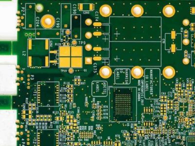
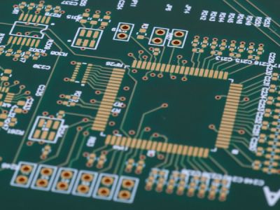
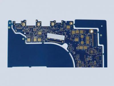
HDI PCB stands for High-Density Interconnect Printed Circuit Board. It is a type of PCB that uses advanced manufacturing techniques and design rules to achieve higher circuit density, smaller size, lighter weight, and better performance than regular PCBs. HDI PCBs are widely used in applications that require high speed, high frequency, low noise, low power consumption, and miniaturization, such as smartphones, tablets, laptops, cameras, medical devices, aerospace equipment, etc.
HDI PCBs typically feature the following characteristics:
- More layers: HDI PCBs can have up to 20 layers or more, compared to regular PCBs that usually have 4 to 10 layers. More layers allow for more routing options and signal integrity.
- Smaller vias: HDI PCBs use microvias, which are vias with a diameter of less than 150 microns. Microvias can be blind (connecting an outer layer to an inner layer), buried (connecting two inner layers), or stacked (connecting multiple layers). Microvias reduce the surface area required for routing and increase the available space for components.
- Thinner lines: HDI PCBs use thinner lines and spaces than regular PCBs. The line width and space can be as small as 76.2 microns or less. Thinner lines reduce the parasitic capacitance and inductance, improving the signal quality and speed.
- Thinner materials: HDI PCBs use thinner dielectric materials than regular PCBs. The dielectric thickness can be as low as 80 microns or less. Thinner materials reduce the signal loss and crosstalk, enhancing the electrical performance and reliability.
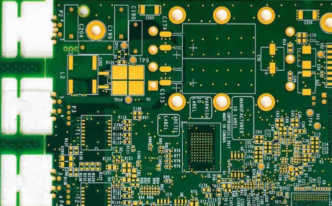
Regular PCB stands for Printed Circuit Board. It is a type of PCB that uses conventional manufacturing techniques and design rules to create circuits on a flat board made of non-conductive material. Regular PCBs are widely used in a variety of electronic devices, from household appliances and industrial machines to automotive systems and musical instruments.
Regular PCBs typically feature the following characteristics:
- Fewer layers: Regular PCBs usually have fewer layers than HDI PCBs. The number of layers depends on the complexity and functionality of the circuit. Fewer layers limit the routing options and signal integrity.
- Larger vias: Regular PCBs use through-hole vias, which are vias with a diameter of more than 150 microns. Through-hole vias connect all the layers of the board. Larger vias occupy more surface area and reduce the available space for components.
- Thicker lines: Regular PCBs use thicker lines and spaces than HDI PCBs. The line width and space can be as large as 254 microns or more. Thicker lines increase the parasitic capacitance and inductance, degrading the signal quality and speed.
- Thicker materials: Regular PCBs use thicker dielectric materials than HDI PCBs. The dielectric thickness can be as high as 200 microns or more. Thicker materials increase the signal loss and crosstalk, reducing the electrical performance and reliability.
HDI PCBs offer several advantages over regular PCBs, such as:
- Smaller size and lighter weight: HDI PCBs can fit more components into a smaller space, reducing the overall size and weight of the electronic device. This is especially beneficial for portable devices that need to be compact and lightweight.
- Better performance and efficiency: HDI PCBs can achieve higher speed, higher frequency, lower noise, lower power consumption, and better thermal management than regular PCBs. This is especially important for high-end devices that need to deliver optimal performance and efficiency.
- Higher reliability and durability: HDI PCBs can withstand harsh environments better than regular PCBs. They have lower failure rates, lower defect rates, lower thermal stress, lower electromagnetic interference (EMI), lower radio frequency interference (RFI), and higher resistance to shock, vibration, moisture, corrosion, etc.
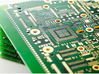
HDI PCB and regular PCB are two different types of printed circuit boards that have different features, applications, and benefits. HDI PCB is a more advanced version of regular PCB that uses microvia technology, thinner lines and materials, and more layers to achieve higher circuit density, smaller size, lighter weight, better performance, higher reliability, and durability than regular PCB. HDI PCB is suitable for high-density applications that require high speed, high frequency, low noise, low power consumption, and miniaturization, such as smartphones, tablets, laptops, cameras, medical devices, aerospace equipment, etc. Regular PCB is a more conventional version of PCB that uses through-hole technology, thicker lines and materials, and fewer layers to create circuits on a flat board. Regular PCB is suitable for low-density applications that do not have strict requirements for performance and efficiency, such as household appliances, industrial machines, automotive systems, musical instruments, etc.
The HDI PCB manufacturing process is more complicated and challenging than the standard PCB manufacturing process. It involves several steps, such as:
- Design: The HDI PCB design must consider the layout, routing, impedance control, signal integrity, thermal management, and reliability issues. The design must also comply with the HDI PCB supplier's capabilities and specifications.
- Material selection: The HDI PCB material must have high dielectric constant, low loss tangent, low coefficient of thermal expansion, high glass transition temperature, and high thermal stability. The material must also be compatible with the microvia formation and filling methods.
- Microvia formation: The microvias are formed by laser drilling or plasma etching through the dielectric layers. The microvias can be filled with conductive or non-conductive materials to improve the mechanical strength and electrical performance of the HDI PCB.
- Lamination: The HDI PCB layers are laminated together using heat and pressure. The lamination process must ensure a good bond between the layers and avoid any defects such as delamination, voids, or misalignment.
- Plating: The HDI PCB surface is plated with copper to form the outer layer traces and pads. The plating process must ensure a uniform and smooth copper layer with good adhesion and solderability.
- Etching: The HDI PCB copper layer is etched to remove the unwanted copper and create the desired circuit pattern. The etching process must ensure a precise and accurate trace width and spacing with minimal undercutting or overetching.
- Solder mask: The HDI PCB solder mask is applied to protect the copper layer from oxidation and corrosion and prevent solder bridging during assembly. The solder mask must have good resolution, adhesion, and heat resistance.
- Surface finish: The HDI PCB surface finish is applied to enhance the solderability and reliability of the solder joints. The surface finish can be electroless nickel immersion gold (ENIG), immersion silver (ImAg), immersion tin (ImSn), organic solderability preservative (OSP), or other types.
- Testing: The HDI PCB is tested for functionality, quality, and performance using various methods such as electrical testing, optical inspection, x-ray inspection, microsection analysis, thermal cycling, etc.
When choosing an HDI PCB factory for your project, you should consider the following factors:
1. Capability: The HDI PCB supplier should have the capability to produce your desired HDI PCB type, layer count, board size, thickness, via size, trace width and spacing, etc. You should check their equipment, technology, and quality standards.
2. Experience: The HDI PCB supplier should have enough experience in producing HDI PCBs for your specific application and industry. You should check their portfolio, certifications, and customer feedback.
3. Service: The HDI PCB supplier should provide you with excellent service throughout the whole process from design to delivery. You should check their communication skills, responsiveness, flexibility, lead time, pricing, etc.
We are a professional HDI PCB manufacturer with over 10 years of experience in the industry. We can provide you with high-quality HDI PCBs that meet your specifications and expectations. Here are some reasons why you should choose us as your HDI PCB assembly partner:
- We have advanced equipment and technology to produce various types of HDI PCBs with high accuracy and efficiency.
- We have a team of skilled engineers and technicians who can assist you with your HDI PCB design and optimization.
- We have a strict quality control system that ensures every HDI PCB is tested and inspected before delivery.
- We have a fast and reliable delivery service that can ship your HDI PCBs to your location in a timely manner.
- We have a competitive and transparent pricing policy that can save you money and time.
If you are interested in our HDI PCB manufacturing and assembly services, please contact us today. We will be happy to provide you with a free quote and consultation. We look forward to hearing from you soon!