Professional China PCB Assembly Online Services
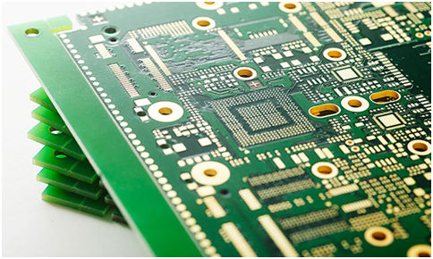
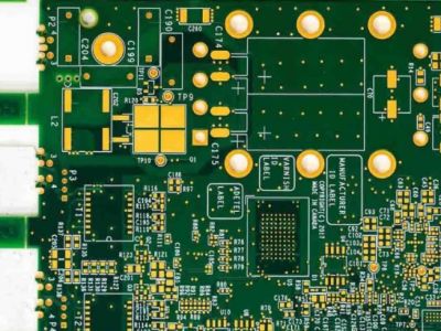
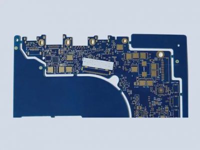
High-Density Interconnect (HDI) PCBs, as the name suggests, are designed to have a higher density of components and interconnections compared to traditional PCBs. The primary goal of HDI technology is to achieve more functionality in a smaller space, making it suitable for compact electronic devices such as smartphones, tablets, and other portable gadgets. Here are some key differences between HDI PCBs and traditional PCBs:
1.Layer Count:
Traditional PCBs often have fewer layers, typically one to four layers. In contrast, HDI PCBs have a higher layer count, commonly ranging from six to more than 20 layers. The increased layer count allows for more routing options and component placement flexibility.
2.Miniaturization:
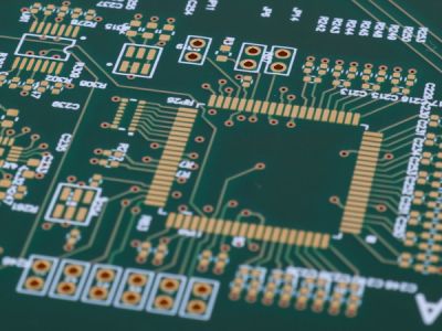
HDI PCBs are designed to accommodate smaller and more tightly packed components. This miniaturization is achieved through techniques like microvias, blind vias, and buried vias. These advanced via technologies allow for more efficient use of space and enable the routing of traces between layers.
3.Vias:
Microvias, blind vias, and buried vias are commonly used in HDI PCBs. Microvias are very small holes that connect different layers of the PCB. Blind vias connect an outer layer to one or more inner layers, while buried vias connect two or more inner layers without extending to the outer layers. These via technologies enable the routing of traces in a more compact and efficient manner.
4.Aspect Ratio:
The aspect ratio of a via is the ratio of its depth to its diameter. HDI PCBs often have higher aspect ratios for their vias compared to traditional PCBs. High aspect ratios allow for deeper vias, facilitating the connection of multiple layers without taking up excessive space.
5.Materials:
HDI PCBs may use advanced materials, such as high-performance laminates and thinner copper foils, to enable finer traces and smaller feature sizes. These materials contribute to the overall miniaturization and improved performance of the HDI PCB.
6.Manufacturing Processes:
The manufacturing processes for HDI PCBs are more complex and involve additional steps compared to traditional PCBs. Precision drilling, laser drilling, and sequential lamination are some of the techniques used in HDI PCB manufacturing.
7.Cost:
HDI PCBs are generally more expensive to manufacture than traditional PCBs due to the increased complexity of the manufacturing processes and the use of advanced materials.
In summary, the construction of HDI PCBsdiffers from traditional PCBs primarily in terms of layer count, miniaturization techniques, via technologies, materials, manufacturing processes, and cost. HDI technology allows for the creation of compact and high-performance PCBs suitable for modern electronic devices with stringent size and weight constraints.