Professional China PCB Assembly Online Services
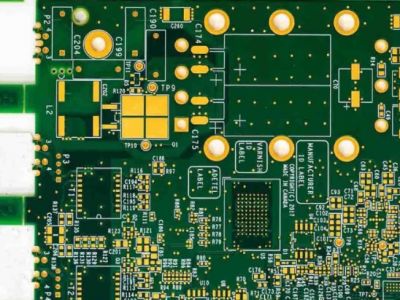
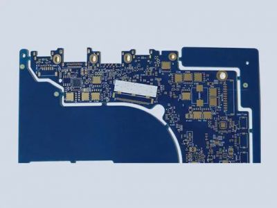
High-Density Interconnect (HDI) PCBs (Printed Circuit Boards) differ from standard PCBs in terms of their complexity and the technologies involved. HDI PCBs are designed to accommodate a higher density of components and connections in a smaller space, which is crucial for modern electronic devices that demand compact and lightweight designs. Here are some key differences in the design process for HDI PCBs compared to standard PCBs:
1. Layer Count and Density:
HDI PCBs typically have a higher layer count compared to standard PCBs. They may involve multiple layers of microvias and buried vias to achieve higher component density.
The increased layer count allows for more complex routing and efficient use of space, enabling designers to pack more components into a smaller area.
2. Microvias:
HDI PCBs often utilize microvias, which are tiny drilled holes with diameters less than 150 micrometers. These microvias enable the routing of traces in high-density areas.
Designing with microvias requires careful consideration of fabrication capabilities, as not all PCB manufacturers can produce boards with extremely small vias.
3. Blind and Buried Vias:
HDI designs frequently incorporate blind and buried vias. Blind vias connect an outer layer to one or more inner layers, while buried vias connect inner layers without penetrating the outer layers. This allows for more efficient use of space on the board.
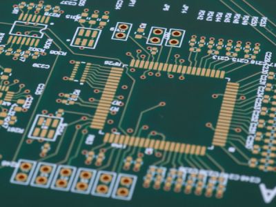
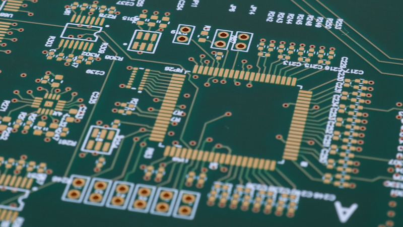
4. Fine Pitch Components:
HDI PCBs often involve the use of fine pitch components with smaller pad and trace sizes. This requires careful attention to manufacturing tolerances and precision during the design process.
5. Advanced Materials:
HDI PCBs may use advanced materials with specific dielectric constants and thermal properties to meet the demands of high-frequency applications and miniaturization.
The selection of materials becomes critical in ensuring signal integrity, controlled impedance, and reliability in high-density designs.
6. Advanced Manufacturing Techniques:
HDI PCBs require advanced manufacturing techniques, such as laser drilling and sequential lamination, to achieve the desired layer stack-up and microvia structures.
Designers need to be familiar with the capabilities and limitations of the chosen manufacturing processes to ensure successful fabrication.
7. Signal Integrity Challenges:
High-density designs may pose challenges related to signal integrity, crosstalk, and electromagnetic interference. Designers must employ best practices for high-speed digital signaling and power distribution.
8. Thermal Management:
Given the smaller form factor and higher component density, thermal management becomes more critical in HDI designs. Designers need to consider heat dissipation and the placement of thermal vias.
In summary, designing HDI PCBsrequires a deeper understanding of advanced manufacturing processes, materials, and technologies to achieve the desired level of miniaturization and component density. Collaboration with experienced PCB manufacturers is crucial to ensuring successful fabrication and assembly of HDI PCBs.