Professional China PCB Assembly Online Services
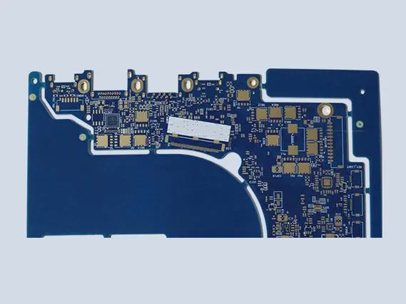
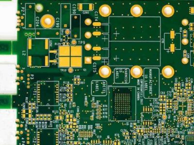
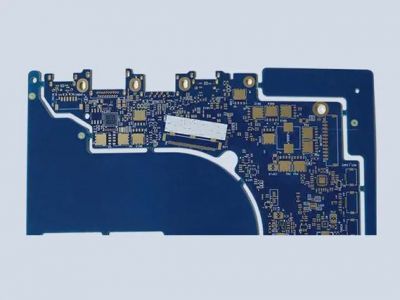
HDI PCB stands for High-Density Interconnect Printed Circuit Board. Its significance in the field of electronics lies in its ability to pack more components and connections into a smaller space compared to traditional printed circuit boards (PCBs). HDI technology enables the creation of intricate circuit designs with finer lines and spaces, smaller vias, and multiple layers, allowing for increased circuit density and miniaturization of electronic devices.
The key features and significance of HDI PCBs include:
Miniaturization: HDI PCBs facilitate the development of smaller and more compact electronic devices, which is crucial for applications where size and weight are critical factors.
Increased Component Density: The technology allows for higher component density and more complex circuitry by utilizing microvias, stacked vias, and fine-pitch components.
Enhanced Performance: HDI PCBs contribute to improved signal integrity, reduced signal loss, and enhanced electrical performance due to shorter interconnection paths and optimized signal routing.
Improved Thermal Management: The compact design of HDI PCBs enables more efficient heat dissipation, contributing to better thermal management in electronic devices.
Reduced Signal Cross-Talk: With the use of advanced technologies such as buried vias and blind vias, HDI PCBs help minimize signal cross-talk and electromagnetic interference.
Support for Advanced Technologies: HDI PCBs are well-suited for advanced technologies such as high-frequency applications, fine-pitch components, and high-speed data transmission, making them essential for modern electronic devices.
Increased Design Flexibility: Designers have greater flexibility in routing traces and placing components, enabling more innovative and sophisticated electronic product designs.
Multi-Layer Structures: HDI PCBs often feature multiple layers, allowing for complex and densely packed circuitry without significantly increasing the overall size of the board.
In summary, HDI PCB technology is a critical enabler for the development of smaller, more powerful, and feature-rich electronic devices, meeting the demands of industries such as consumer electronics, telecommunications, medical devices, and automotive electronics.