
Professional China PCB Assembly Online Services
 September 20, 2023
Evaluating multilayer PCB manufacturers for quality and reliability is crucial when selecting a partner for your electronics projects. Here is a comprehensive guide on how to assess and choose the rig
Continue Reading.... September 19, 2023
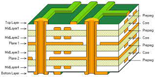
Multilayer PCB design in Altium Designer is a comprehensive process that involves creating a multilayered printed circuit board with precise control over layer stackup, component placement, signal rou
Continue Reading.... September 17, 2023
High-Density Interconnect (HDI) PCB manufacturing requires strict quality control to ensure the reliability and functionality of these complex circuit boards. Here are some key quality control measure
Continue Reading.... September 16, 2023
High-Density Interconnect Printed Circuit Boards (HDI PCBs) have gained significant popularity in recent years due to their ability to accommodate complex electronic designs in compact form factors. T
Continue Reading....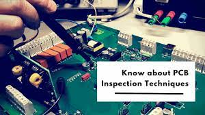 September 15, 2023
To ensure the quality and functionality of HDI PCBs, thorough inspection techniques are essential during the manufacturing process. This article will delve into the various HDI PCB inspection techniqu
Continue Reading.... September 14, 2023
High-Density Interconnect (HDI) printed circuit boards (PCBs) have become a crucial component in modern electronic devices, thanks to their ability to accommodate more functionality in smaller form fa
Continue Reading....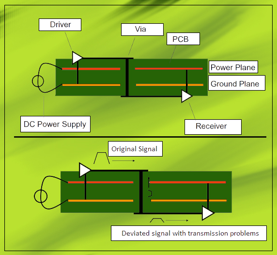 September 13, 2023
With the ever-increasing demand for faster data rates and more complex electronic systems, ensuring signal integrity in HDI PCB layout has become a critical challenge. This article will explore the ke
Continue Reading.... September 12, 2023
High-Density Interconnect (HDI) printed circuit boards (PCBs) have become increasingly prevalent in modern electronics due to their compact size and improved performance. However, with the ever-increa
Continue Reading....
September 11, 2023
High-Density Interconnect (HDI) Printed Circuit Boards (PCBs) have become a fundamental component in modern electronic devices due to their compact size and increased component density. Achieving high
Continue Reading.... September 10, 2023
High-Density Interconnect (HDI) PCBs have become a staple in modern electronics due to their ability to accommodate densely packed components and intricate designs. This article delves into the critic
Continue Reading....
September 9, 2023
Hybrid HDI (High-Density Interconnect) PCB designs have gained significant popularity in recent years due to their ability to accommodate complex electronic components and miniaturized devices. This a
Continue Reading....
September 8, 2023
In the realm of printed circuit boards (PCBs), High-Density Interconnect (HDI) technology has paved the way for enhanced performance and miniaturization. Two prominent approaches within the HDI catego
Continue Reading....


