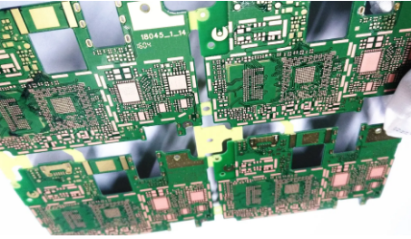
High-Density Interconnect (HDI) Printed Circuit Boards (PCBs) have become a fundamental component in modern electronic devices due to their compact size and increased component density. Achieving high-density routing in HDI PCBs requires the implementation of specialized techniques and methods. In this article, we will explore various strategies for optimizing the layout and routing of HDI PCBs to meet the demands of today's electronics industry.

1. Multilayer Design:
HDI PCBs typically employ multilayer designs, with internal layers used for via interconnections, reducing the number of components on the surface layers. This enhances the PCB's layout density.
2. Microvias:
The use of microvias, such as blind vias and buried vias, enables electrical connections between different layers. These vias are typically much smaller than traditional through-holes, allowing for a higher component count.
3. Fine Line Widths and Spacings:
Utilizing narrower trace widths and smaller spacings accommodates more traces in limited space. Microtrace widths and spacings are often employed to achieve high-density routing.
4. Stacking Techniques:
Stacking multiple thin boards together to form a thinner yet multi-layer PCB increases interconnect density. This often involves using bonding materials to laminate different layers.
5. Surface Mount Technology (SMT):
The use of miniature surface-mount components, such as BGA packages, and micro SMT, further enhances component density on the PCB surface.
6. Advanced Design Tools:
Advanced PCB design software aids in efficient layout planning, routing, and component placement to ensure the successful implementation of high-density routing.
7. Impedance Control:
For high-frequency applications, maintaining impedance control is crucial. Special materials and routing techniques are employed to ensure signal integrity and performance.
8.Analog and Mixed-Signal Design:
In HDI PCBs, analog and digital signals may coexist, necessitating careful consideration of signal isolation and interference suppression.
9.Precision Manufacturing Processes:
The manufacture of high-density PCBs demands high-precision processing to ensure the accurate fabrication of tiny vias and traces.
10.Testing and Inspection:
After manufacturing and assembly, thorough testing and inspection are essential to verify the absence of manufacturing defects and electrical issues.
High-density routing techniques are critical for the successful design and fabrication of HDI PCBs, meeting the requirements of modern electronic devices for compactness, lightweight, and high performance. However, it is essential to carefully assess project needs and budgets, as high-density PCB design and manufacturing often involve increased costs and technical requirements.
Get more knowledge about High-Density Routing Techniques for HDI PCBs please refer to Rigaopcb:https://www.rigaopcb.com/