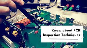
To ensure the quality and functionality of HDI PCBs, thorough inspection techniques are essential during the manufacturing process. This article will delve into the various HDI PCB inspection techniques employed in the industry.

1.Automated Optical Inspection (AOI):
Automated Optical Inspection is a widely used technique for inspecting HDI PCBs. It involves the use of high-resolution cameras and advanced image processing software to detect defects such as soldering issues, component misalignment, and missing components. AOI can quickly scan PCBs and provide detailed reports, making it an efficient method for high-volume production.
2.X-ray Inspection:
X-ray inspection is invaluable for examining the inner layers of HDI PCBs, which often contain multiple stacked vias and intricate traces. This non-destructive technique allows inspectors to identify defects like voids in solder joints, delamination, and shorts between PCB layers. X-ray inspection is especially crucial for ensuring the integrity of fine-pitch components.
3.Automated X-ray Inspection (AXI):
Automated X-ray Inspection takes X-ray inspection a step further by automating the process. It utilizes robotic arms and specialized software to precisely position the PCB and capture X-ray images. AXI can detect defects that may be missed by manual X-ray inspection due to its higher accuracy and repeatability.
4.In-Circuit Testing (ICT):
In-Circuit Testing involves the use of specialized fixtures and test probes to verify the electrical functionality of individual components and connections on the HDI PCB. While ICT is effective in identifying electrical defects, it may not detect issues related to passive components or open vias.
5.Flying Probe Testing:
Flying Probe Testing is a versatile technique that employs automated test probes to check the connectivity and functionality of PCB components. It is particularly useful for prototypes and low-volume production runs, as it doesn't require the creation of custom fixtures. Flying probe testers can access hard-to-reach areas on densely populated HDI PCBs.
6.Thermal Imaging:
Thermal imaging is employed to detect issues related to temperature variations on HDI PCBs. Hot spots can indicate electrical shorts, component overheating, or inadequate thermal dissipation. Thermal imaging cameras capture heat signatures, allowing inspectors to pinpoint potential problems before they cause failures.
Cross-Sectional Analysis:
Cross-sectional analysis involves cutting and polishing a sample of the HDI PCB to inspect its internal structure under a microscope. This technique is particularly valuable for assessing the quality of plated vias, dielectric materials, and the alignment of stacked layers. Cross-sectional analysis provides detailed insights into the PCB's construction.
Conclusion:
Ensuring the reliability and performance of High-Density Interconnect Printed Circuit Boards is critical for the success of modern electronic devices. Employing a combination of inspection techniques, such as Automated Optical Inspection, X-ray Inspection, In-Circuit Testing, and others, manufacturers can identify and rectify defects in HDI PCBs, thereby delivering high-quality products to consumers. These inspection techniques play a crucial role in maintaining the integrity of electronic systems in various applications.
Get more knowledge about HDI PCB Inspection Techniques please refer to Rigaopcb:https://www.rigaopcb.com/