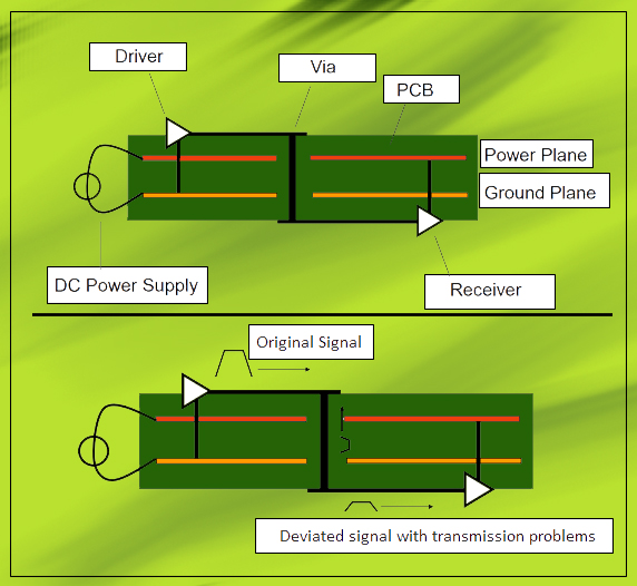
With the ever-increasing demand for faster data rates and more complex electronic systems, ensuring signal integrity in HDI PCB layout has become a critical challenge. This article will explore the key considerations and best practices for maintaining signal integrity in HDI PCB designs.

1.Controlled Impedance:
One of the fundamental aspects of signal integrity is controlling impedance. In HDI PCBs, signal traces are often narrower and closer together, which can affect impedance characteristics. To maintain controlled impedance, designers must carefully select the dielectric materials and stack-up configurations to match the required impedance values for high-speed signals. Simulations and impedance calculators can be invaluable tools in achieving this.
2.Signal Routing:
In HDI PCBs, the density of components and interconnections can lead to complex routing scenarios. It's essential to pay close attention to the routing of high-speed signals. Differential pairs should be routed closely together with consistent spacing, and care should be taken to avoid sharp corners and right-angle traces, which can introduce signal reflections and crosstalk.
3.Signal Return Paths:
The return path for high-speed signals is equally important as the signal trace itself. To minimize ground bounce and signal integrity issues, designers should create low-impedance return paths, often by using ground planes or stitching vias. Proper decoupling capacitors should also be placed strategically near high-speed components to provide a stable return path.
4.Crosstalk Mitigation:
Crosstalk is a common challenge in HDI PCB layouts due to the proximity of traces. To mitigate crosstalk, designers can implement techniques such as differential signaling, guard traces, and ground shielding. Careful placement and routing of critical signals can also help reduce the risk of crosstalk.
5.Signal Termination:
Proper termination is crucial for high-speed signals. Series termination resistors or parallel termination schemes can be employed to match the signal source's output impedance and reduce signal reflections. The choice of termination method should align with the specific requirements of the HDI PCB design.
6.Signal Integrity Analysis:
Signal integrity analysis tools like SPICE simulations and electromagnetic field solvers can aid in evaluating the performance of HDI PCB layouts. These tools help identify potential signal integrity issues, such as impedance mismatches, reflections, and overshoot/undershoot, allowing designers to make necessary adjustments before prototyping.
7.Design for Manufacturability:
Finally, it's essential to consider the manufacturability of the HDI PCB design. As the complexity increases, the fabrication process becomes more critical. Collaborating closely with PCB manufacturers can help ensure that the chosen materials and fabrication techniques are compatible with the desired signal integrity goals.
Signal integrity is a paramount concern in HDI PCB layout, especially as electronics continue to push the boundaries of speed and density. By carefully considering controlled impedance, signal routing, return paths, crosstalk mitigation, termination, and thorough analysis, designers can create HDI PCBs that meet the demands of high-speed applications while maintaining signal integrity and reliability. Collaboration between design and manufacturing teams is crucial to achieving optimal results in HDI PCB design.
Get more knowledge about Signal Integrity in HDI PCB Layout please refer to Rigaopcb:https://www.rigaopcb.com/