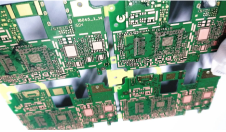
High-Density Interconnect (HDI) printed circuit boards (PCBs) have become increasingly prevalent in modern electronics due to their compact size and improved performance. However, with the ever-increasing power densities of electronic components, effective thermal management in HDI PCB design is crucial to ensure the reliability and longevity of electronic devices. This article delves into the importance of thermal management in HDI PCB design and explores various strategies to address thermal challenges.

The Significance of Thermal Management: Thermal management is vital because excessive heat can lead to several adverse effects, including component failure, reduced performance, and even safety hazards. HDI PCBs, with their densely packed components and narrow traces, are particularly susceptible to heat buildup. Without proper thermal management, these boards can experience hotspots, which can compromise the functionality and durability of the PCB and its components.
Strategies for Thermal Management in HDI PCB Design:
Component Placement and Orientation:
Careful placement of heat-generating components can help distribute heat more evenly across the PCB. Placing heat-sensitive components away from hotspots is essential.
Orienting components to maximize airflow and minimize heat buildup is crucial. Consider using thermal analysis tools to optimize component placement.
Heat Sinks and Thermal Pads:
The use of heat sinks and thermal pads can effectively dissipate heat from high-power components. Properly sized and designed heat sinks can significantly reduce component temperatures.
Thermal pads provide a thermal bridge between components and the PCB, enhancing heat transfer. Ensure proper material selection for thermal pads.
Copper Thickness and Traces:
Increasing the copper thickness in PCB layers can enhance heat dissipation. Thicker copper layers have lower thermal resistance, allowing for better heat flow.
Wider traces and vias can help reduce resistance and improve thermal conductivity, allowing heat to disperse more efficiently.
Thermal Vias:
Thermal vias connect different PCB layers to facilitate heat transfer. Placing thermal vias strategically beneath heat sources can help conduct heat away from critical areas.
The use of microvias and blind vias allows for more precise thermal management without compromising the PCB's density.
PCB Substrate Material:
Choosing the right PCB substrate material with high thermal conductivity, such as metal-core PCBs, can enhance heat dissipation.
Consider materials like FR-4 or polyimide with high-temperature ratings for improved thermal performance.
Thermal Simulation and Testing:
Utilize thermal simulation software to analyze and predict heat distribution within the HDI PCB. This aids in identifying potential hotspots and optimizing the design.
Conduct thermal testing and measurements to validate the effectiveness of the thermal management solutions employed.
In the realm of HDI PCB design, thermal management is a critical consideration to ensure the reliability and performance of electronic devices. By strategically implementing component placement, heat sinks, copper thickness, thermal vias, appropriate substrate materials, and thorough thermal analysis, designers can effectively mitigate thermal challenges and create high-performance HDI PCBs that meet the demands of modern electronics. Prioritizing thermal management not only extends the lifespan of electronic products but also enhances their overall quality and safety.
Get more knowledge about Thermal Management in HDI PCB Design please refer to Rigaopcb:https://www.rigaopcb.com/