Professional China PCB Assembly Online Services
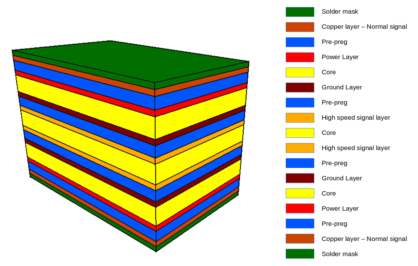
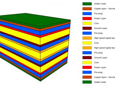
Multilayer printed circuit boards (Multilayer PCBs) offer several advantages in electronic designs, making them a popular choice for a wide range of applications. Here are some of the key advantages of using multilayer PCBs:
1.High Component Density:
Multilayer PCBs allow for a higher component density because they have multiple layers of copper traces and insulating material. This enables more compact and complex electronic designs, ideal for miniaturized devices and densely populated circuit boards.
2.Improved Signal Integrity:
Multilayer PCBs support controlled impedance routing, which is crucial for high-speed digital and RF (radio frequency) circuits. This ensures that signals maintain their integrity, reducing signal degradation, reflection, and crosstalk.
3.Enhanced Power Distribution:
Multilayer PCBs provide dedicated power and ground planes, improving power distribution and reducing voltage drops and noise. This is particularly important in circuits with multiple power domains or high-power components.
4.Reduced EMI/RFI:
Multilayer boards can be designed with ground and power planes to act as shields, reducing electromagnetic interference (EMI) and radio-frequency interference (RFI). This is critical in applications where electromagnetic compatibility (EMC) is a concern.
5.Complex Routing:
Multilayer PCBs allow for intricate and high-density routing of signal traces. This is especially valuable for designs with a large number of interconnected components or complex signal paths.
6.Enhanced Thermal Management:
Additional copper layers can be used as heat sinks or for thermal vias to dissipate heat from hot components, improving thermal management and preventing overheating.
7.Improved Reliability:
Multilayer boards offer better reliability due to the reduced risk of signal interference, reduced thermal stress, and fewer signal via transitions. This can lead to longer-lasting and more robust electronic systems.
8.Space Savings:
Multilayer PCBs can reduce the overall size of the board, which is especially important in applications where space is limited or where compact design is a priority.
9.Design Flexibility:
Multilayer PCBs provide greater design flexibility, allowing for more efficient use of available space and enabling advanced features and capabilities in electronic devices.
10.Ease of Routing Changes:
When design changes are needed, it's often easier to make adjustments in multilayer PCBs compared to single or double-layer boards, which can require more significant redesign.
11.Support for Advanced Technologies:
Many modern electronic applications, such as high-performance computing, IoT devices, and mobile communication devices, rely on multilayer PCBs to support advanced functionalities and connectivity.
12.Higher-Performance Capabilities:
Multilayer PCBs are essential for applications where performance is critical, such as high-frequency circuits, high-speed digital designs, and applications that require a high signal-to-noise ratio.
While multilayer PCBs offer many advantages, they also come with increased design complexity, cost, and manufacturing challenges. Engineers should carefully evaluate the specific requirements of their electronic designs to determine whether a multilayer PCB is the best choice for their application.
Get more knowledge about the advantages of using a multilayer PCB in electronic designs please refer to Rigaopcb:https://www.rigaopcb.com/