Professional China PCB Assembly Online Services
In this guide, we'll explain how to make multilayer PCBs (printed circuit boards) in a simple way. We'll cover everything from the basic steps to the more complicated parts of the process. This article is helpful for both beginners and those who already know a bit about PCB manufacturing. We aim to give you useful tips and insights on how to properly make multilayer PCBs.
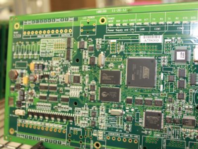
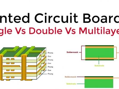
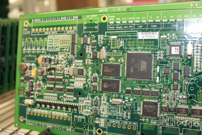
Multilayer PCBs, or multilayer printed circuit boards, are complicated parts used in many devices. Multilayer PCBs are different from ones with only one layer or two sides because they have many copper layers. These layers stick together with a glue-like substance called epoxy resin. The layers are linked by holes filled with metal. This setup allows for complicated wiring and ways for electrical signals to move through.
Multilayer PCBs offer several advantages over single layer PCBs or double sided PCBs. Firstly, they provide increased circuit density, allowing for compact designs in applications where space is limited. This compactness can be vital in modern electronic devices such as smartphones and wearables, where miniaturization is key.
Additionally, multilayer PCBs offer enhanced electrical performance. With the use of multiple layers, designers can optimize the signal paths and minimize signal interference, resulting in improved signal integrity and reduced electromagnetic interference (EMI). This leads to more reliable and efficient electrical systems.
Multilayer PCBs come in various types, depending on the number of layers and their configurations. The most common types include:
4-Layer PCBs: These consist of four layers (two internal layers and two outer layers) and are widely used for moderately complex electronic systems.
6-Layer PCBs: With six layers (four internal layers and two outer layers), these multilayer printed circuit boards are suitable for applications requiring higher complexity and denser circuitry.
8-Layer PCBs: As the complexity of the electronic system increases, eight-layer PCBs provide more flexibility and better performance with six internal layers and two outer layers.
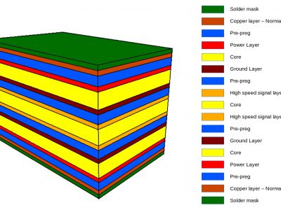
Multi layer PCB stack: A multi layer stack refers to the arrangement of multiple layers of copper foil and laminates in a multilayer PCB board.
The multilayer PCB manufacturing process involves several stages, ensuring the precise alignment of layers and the creation of reliable and high-quality multilayer PCBs. Let's explore each step in detail:
The first step in the multilayer PCB manufacturing process is designing the PCB layout. Using specialized software, designers create the circuit schematic and define the placement of components. Proper planning and optimization during this stage are vital to the success of the pcb board's manufacturing process.
Selecting the appropriate materials is crucial for the multilayer PCB manufacturing process. The choice of laminate materials, copper foils, and epoxy resins depends on factors such as thermal and electrical conductivity, dielectric strength, and cost considerations. Careful material selection ensures the desired performance and reliability of the final multilayer PCB.
Next, precision drilling is performed to create holes for plated through holes and component leads. Smaller plated through holes enable more complex circuitry. Drilling the holes, we plate them with a conductive material, typically copper, to establish electrical connections between the layers.
In this part of making a printed circuit board (pcb), we add a light-sensitive layer called a solder mask on top of the copper. Then, we use ultraviolet light to project the circuit board design onto the solder mask. The light removes the uncovered parts, and we're left with the copper paths and circuit designs we want.
First, the different layers are made ready. Then, they are stacked and glued together with a special glue called epoxy resin and heat. This gluing method makes sure the layers can conduct electricity between them and also makes the multilayer PCB strong.
To protect the copper traces and pads from oxidation, a surface finish is applied to the outer layers. This also assists with solderability during the assembly process. Common surface finishes for multilayer PCBs include HASL (Hot Air Solder Leveling), ENIG (Electroless Nickel Immersion Gold), and immersion tin.
Quality control is crucial in the multilayer PCB manufacturing process. Automated optical inspection (AOI) and X-ray testing are commonly used to detect any potential defects or anomalies in the board. This step ensures that the multilayer PCB meets the required standards and specifications.
After inspection, the manufactured multilayer PCBs undergo rigorous electrical tests. This involves checking the continuity, impedance, and functionality of the circuitry to verify that the PCB performs as expected.
After successful tests, the multilayer PCBs are cut into separate pieces. Then, they go through any extra steps needed, such as routing, scoring, or tab-routing. The completed panels are then ready for assembly.
Multilayer PCB manufacturing comes with its fair share of challenges. Understanding and addressing these challenges are essential for achieving optimal results. Here are a few common challenges faced:
Aligning the layers accurately during the bonding process can be challenging. Misalignments can cause impedance mismatches or even board failure. Manufacturers employ precision machinery and techniques to minimize alignment issues.
Choosing the right laminate material is critical to ensure the desired electrical and mechanical properties of the multilayer PCB. To prevent issues such as bending and poor signal quality, we must think about how materials stretch when they get hot and how well they conduct electricity.
As the complexity of multilayer PCBs increases, maintaining signal integrity becomes more challenging. Engineers need to carefully watch how signals move, how energy is spread out, and how gadgets are hooked up to the ground.This is important to avoid issues such as signals getting mixed up, unwanted noise, and electromagnetic interference.
The field of multilayer PCB manufacturing is constantly evolving. Emerging trends and technologies are shaping the industry for improved performance, efficiency, and reliability. These include:
High-frequency multilayer PCBs for applications like 5G and wireless communication systems.
Flexible multilayer PCBs, enabling bendable and foldable electronic devices.
Advanced materials with enhanced thermal, mechanical, and electrical properties, such as ceramic-based laminates.
While multilayer PCB manufacturing can be intricate, adhering to certain guidelines can help ensure successful outcomes. Here are a few tips to consider:
Collaborate closely with PCB designers to optimize the layout and reduce complexity.
Choose high-quality materials, such as copper foils and epoxy resins, that meet the specific requirements of the application.
Regularly calibrate and maintain manufacturing equipment to minimize errors and inconsistencies.
Perform thorough testing and inspection at each stage, including electrical tests, to catch any potential issues early on.
Stay informed about the latest industry developments to leverage new techniques and technologies.
Multilayer PCB manufacturing is a complex and fascinating process that lies at the heart of modern electronic systems. Understanding the intricacies and challenges involved is crucial for producing reliable and high-performance circuit boards. If you follow this guide's steps and stay updated with the newest trends in the industry, you'll find it simpler to handle making multilayer PCBs.
The manufacturing time for multilayer PCBs varies depending on several factors, including complexity, quantity, and equipment availability. Generally, it can take anywhere from a few days to a few weeks to complete the manufacturing process.
A multilayer Printed Circuit Board (PCB) does not have a strict maximum number of layers. However, industry standards often set this range between 4 and 16 layers. However, some advanced applications may require even higher layer counts.
Multilayer PCBs often cost more because they use more materials and are harder to make. But, they are usually worth the extra money because they make circuits denser, signals clearer, and devices smaller.
Repairing multilayer PCBs can be challenging, especially if the defect affects internal layers. In most cases, it is more cost-effective to replace the faulty board rather than attempting repairs. Proper testing and inspection during manufacturing can help minimize the chances of defects.
Manufacturers typically conduct electric
al tests on each individual layer of a multilayer PCB during the production process. They do these tests to find any open or short circuits in the layers and make sure the circuit works right.
Epoxy resin is a crucial component in the multilayer PCB manufacturing process. It provides adhesive properties during the layer bonding stage, ensuring electrical connectivity between the layers. Epoxy resin also offers mechanical strength, protecting the circuitry from environmental factors and preventing delamination.
Yes, many-layered PCBs can work with high power if designed well. Using thicker copper, wider paths, and good cooling methods helps them handle more power. These designs stop too much heat and power loss, making sure the devices work safely and well.
Finding a reliable multilayer PCB manufacturer is essential for a successful manufacturing process. Here are a few tips to help you find the right one:
Research and shortlist multiple manufacturers based on their experience, certifications, and customer reviews.
Request samples and evaluate the quality of their previous work.
Assess their manufacturing capabilities, equipment, and quality control processes.
Inquire about their prototyping and production lead times, as well as their customer support services.
Discuss your specific requirements and ensure that the manufacturer can meet them within your budget.
By doing these steps and checking carefully, you can find a good PCB maker that fits what you need.
Multilayer PCB manufacturing is a complex and precise process that requires attention to detail and adherence to industry standards. To make good multilayer PCBs, learn the steps, solve problems, and stay updated with new tech. Working with a trusted maker and always learning will help you do well in making multilayer PCBs.