Professional China PCB Assembly Online Services

Multilayer PCBs have become a cornerstone in the realm of electronic design, offering a sophisticated solution to the complexities of modern electronics. Let's embark on a journey to unravel the nuances of Multilayer PCBs, exploring their definition, manufacturing intricacies, and a myriad of applications that leverage their advanced capabilities.
1.What is the definition of a Multilayer PCB?
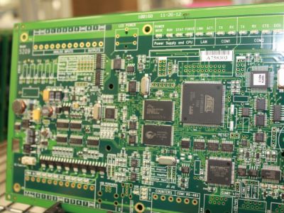
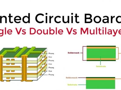
A Multilayer PCB, or Multilayer Printed Circuit Board, is a type of printed circuit board that features multiple layers of conductive copper foil separated by layers of insulating material. Unlike single-layer or double-layer PCBs, which have conductive traces on only one or both sides, a Multilayer PCB incorporates multiple layers, allowing for a more complex and dense circuit design. The layers are interconnected through plated holes, forming a three-dimensional circuit structure. Multilayer PCBs are widely used in electronic devices where space constraints and intricate circuitry demand a higher level of integration and functionality.

2.benefits and applications of Multilayer PCBs
Benefits of Multilayer PCBs:
Higher Density and Complexity: Multilayer PCBs allow for a more compact design with increased component density, enabling the integration of complex circuits in a smaller space.
Enhanced Signal Integrity: The multiple layers help minimize signal interference and noise, leading to improved signal integrity and overall performance.
Reduced Electromagnetic Interference (EMI): With proper design, the multiple layers can act as shielding, reducing electromagnetic interference and ensuring reliable operation.
Improved Power Distribution: Multilayer PCBs facilitate efficient power distribution, reducing the risk of voltage drops and ensuring consistent power supply to components.
Greater Design Flexibility: Designers have more flexibility in routing traces and placing components, leading to more creative and efficient circuit designs.
Higher Component Count: Multilayer PCBs can accommodate a larger number of components, making them suitable for applications requiring a multitude of functionalities.
Increased Reliability: The redundancy of connections and the ability to distribute components across layers enhance the overall reliability of the circuit.
Applications of Multilayer PCBs:
Consumer Electronics: Widely used in smartphones, tablets, laptops, and other consumer electronic devices where miniaturization and high functionality are crucial.
Telecommunications Equipment: Multilayer PCBs are integral components in communication devices, base stations, and networking equipment due to their ability to handle complex signal processing.
Medical Devices: In medical electronics, where precision and compact designs are essential, Multilayer PCBs find applications in devices like medical imaging equipment and diagnostic devices.
Automotive Systems: Used in automotive control units, navigation systems, and advanced driver-assistance systems (ADAS) to meet the demand for compact and reliable electronic components.
Industrial Equipment: Multilayer PCBs play a key role in the control systems of industrial machinery, providing the necessary complexity and reliability.
Aerospace and Defense: Commonly used in avionics, radar systems, and defense applications where compact and reliable circuitry is crucial for mission-critical operations.
Computing Systems: Found in servers, high-performance computing systems, and data storage devices, Multilayer PCBs contribute to efficient data processing and storage.
Networking Equipment: Used in routers, switches, and other networking devices to handle the complex communication protocols and high-speed data transfer.
Multilayer PCBs have become essential in various industries, catering to the demand for compact, high-performance electronic devices with advanced functionalities.

3.How are Multilayer PCBs designed and manufactured?
Design of Multilayer PCBs:
Schematic Design: Engineers create a schematic diagram of the circuit, defining the components, connections, and their functions.
Component Placement: Components are placed on the PCB layout, considering factors such as signal integrity, thermal management, and space constraints.
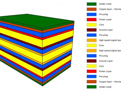
Layer Stackup: Designers determine the layer stackup, specifying the arrangement of copper layers and insulating materials. This decision impacts signal integrity and overall performance.
Routing: Traces are routed to connect components while considering factors like impedance control, signal integrity, and avoiding interference.
Ground and Power Planes: Ground and power planes are incorporated into the design to provide stable reference voltages, minimize noise, and enhance signal integrity.
Via Placement: Vias (plated holes) are strategically placed to connect traces between different layers. Vias play a crucial role in enabling the multilayer structure.
Design Verification: The design undergoes thorough verification using simulation tools and design rule checks to ensure functionality and manufacturability.
Manufacturing of Multilayer PCBs:
Layer Preparation: Thin copper foils are bonded to the substrate material (usually fiberglass-reinforced epoxy) to create individual copper-clad layers.
Drilling: Precision drilling is performed to create holes for vias that will interconnect the different layers. The holes are then coated with a conductive material.
Layer Alignment: The individual layers are aligned and stacked according to the predetermined layer stackup, with insulating material between them.
Lamination: The layered structure undergoes lamination, where heat and pressure are applied to bond the layers together, forming a single, cohesive unit.
Copper Etching: Excess copper is etched away, leaving only the desired traces and copper areas on each layer.
Plating and Surface Finish: Additional copper plating is applied to the exposed vias, and the board's surface is coated with a finish to protect it from oxidation and facilitate soldering.
Solder Mask Application: A solder mask is applied to cover areas where solder should not be applied, protecting the board and aiding in component soldering.
Silkscreen Printing: Component designators, logos, and other markings are added using silkscreen printing for identification and assembly guidance.
Testing: The finished Multilayer PCB undergoes testing, including electrical testing, to ensure that all connections are functional and the board meets quality standards.
Final Inspection: The PCB undergoes a final inspection for defects, ensuring that it meets the design specifications and quality standards.
The design and manufacturing of Multilayer PCBs involve a meticulous process that combines engineering expertise, advanced technology, and precision manufacturing techniques to achieve the desired functionality and reliability.

4.The working of PCB Multilayer Press
The PCB Multilayer Press is a critical component in the manufacturing process of Multilayer PCBs, responsible for creating the layered structure that defines these advanced circuit boards. Here's an overview of the working of a PCB Multilayer Press:
Layer Stacking: The process begins with the preparation of individual layers, typically consisting of copper foils bonded to substrate materials like fiberglass-reinforced epoxy. These layers, often referred to as cores or prepregs, contain conductive traces on their surfaces.
Alignment: The individual layers are carefully aligned according to the predetermined layer stackup. This step is crucial to ensure precision and accuracy in the final Multilayer PCB.
Insertion of Prepregs: Prepregs, which are layers of uncured resin and reinforcing fabric, are inserted between the copper-clad layers. The prepregs act as insulating layers that will solidify during the pressing process.
Tooling and Registration: The layered stack is placed in a specialized tooling or registration system that ensures the accurate alignment of the layers. This tooling helps maintain the layer registration throughout the pressing process.
Pressing Process: The layered stack, along with the prepregs, is subjected to heat and pressure within the Multilayer Press. This process is designed to bond the layers together permanently. The heat activates the resin in the prepregs, causing them to cure and adhere to the copper layers, creating a solid and integrated structure.
Curing: The pressing process includes a curing phase where the resin in the prepregs solidifies, establishing a strong and durable bond between the layers. This phase is essential for the structural integrity of the Multilayer PCB.
Cooling: After the pressing and curing phases, the pressed stack undergoes a controlled cooling process. This step is crucial to ensure that the layers solidify and bond effectively.
Final Inspection: The pressed Multilayer PCB undergoes a final inspection to check for any defects or imperfections in the bonding process. This may include visual inspection, automated optical inspection (AOI), or other quality control measures.
The working of a PCB Multilayer Press is a precise and controlled process that plays a pivotal role in creating the complex and compact structures required for Multilayer PCBs. The ability to stack and bond multiple layers with accuracy is essential for achieving the desired electrical and mechanical characteristics of these advanced circuit boards.
5.When and under what circumstances should multi-layer PCBs be used?
Multilayer PCBs are beneficial in various circumstances, particularly when specific design and performance requirements need to be met. Here are situations where the use of multilayer PCBs is advantageous:
High-Density Circuits: When a circuit design requires a high component density and intricate interconnections that cannot be accommodated on single-layer or double-layer PCBs, multilayer PCBs are preferred.
Signal Integrity: Applications that demand excellent signal integrity, such as high-frequency communication devices, benefit from the reduced signal interference and noise isolation provided by multilayer PCBs.
Miniaturization: In compact electronic devices, where space is limited, multilayer PCBs enable designers to achieve smaller form factors while maintaining or enhancing functionality.
Power Distribution: Multilayer PCBs are effective for distributing power efficiently across the circuit, minimizing voltage drops and ensuring consistent power delivery to all components.
Complex Functionality: For electronic devices with complex functionalities, advanced features, or multiple subsystems, multilayer PCBs provide the necessary structure to integrate diverse components and functions.
Impedance Control: Applications with specific impedance requirements, such as high-speed data transmission systems or RF (radio frequency) circuits, benefit from the controlled impedance characteristics achievable with multilayer PCBs.
High-Speed Data Transfer: Multilayer PCBs are suitable for applications involving high-speed data transfer, as they offer reduced signal distortion and better signal integrity, essential for maintaining data accuracy.
Advanced Manufacturing Technologies: When utilizing advanced manufacturing technologies such as surface mount technology (SMT) or ball grid array (BGA) components, multilayer PCBs provide the necessary space and interconnectivity for these technologies.
Reliability and Redundancy: For applications where reliability is critical, multilayer PCBs offer redundancy in connections and enhance the overall reliability of the circuit. This is particularly important in mission-critical systems.
Thermal Management: Electronic devices generating significant heat can benefit from multilayer PCBs, as they provide additional layers for thermal dissipation, helping manage and distribute heat more effectively.
Mixed-Signal Circuits: Applications that involve both analog and digital signals, such as audio systems or mixed-signal processing devices, benefit from the isolation and reduced crosstalk provided by multilayer PCBs.
In summary, multilayer PCBs are best suited for applications that require compact designs, high component density, enhanced signal integrity, and specific performance characteristics. The decision to use multilayer PCBs depends on the specific needs and requirements of the electronic device being designed.
6.The advantages and disadvantages of Multilayer PCBs?
Advantages of Multilayer PCBs:
High Component Density: Multilayer PCBs allow for a higher density of electronic components, enabling more complex and advanced circuit designs.
Compact Size: The ability to stack multiple layers in a single board allows for compact designs, making multilayer PCBs ideal for applications with limited space.
Enhanced Signal Integrity: Reduced electromagnetic interference and noise make multilayer PCBs suitable for applications where signal integrity is critical, such as high-frequency communication devices.
Improved Power Distribution: Efficient power distribution is achieved through dedicated power and ground planes, minimizing voltage drops and ensuring consistent power delivery.
Design Flexibility: Designers have more flexibility in routing traces and placing components, leading to creative and efficient circuit designs.
Redundancy and Reliability: The redundancy of connections and additional layers contribute to the overall reliability of multilayer PCBs, reducing the risk of circuit failure.
Impedance Control: Multilayer PCBs allow for precise control of impedance, making them suitable for high-speed data transmission and RF applications.
Thermal Management: Additional layers provide space for thermal dissipation, aiding in the effective management of heat generated by electronic components.
Mixed-Signal Applications: Multilayer PCBs are well-suited for mixed-signal applications, providing isolation between analog and digital components to minimize crosstalk.
Higher Complexity: Multilayer PCBs support the integration of multiple subsystems and functionalities within a single board, allowing for the creation of sophisticated electronic devices.
Disadvantages of Multilayer PCBs:
Cost: Multilayer PCBs can be more expensive to manufacture compared to single or double-layer boards, primarily due to the complexity of the manufacturing process.
Complex Manufacturing: The manufacturing process for multilayer PCBs is more intricate and requires advanced techniques, increasing the likelihood of manufacturing challenges.
Repair Difficulty: Repairing a multilayer PCB is more challenging than repairing single or double-layer boards, as accessing and identifying specific layers can be complex.
Increased Lead Time: The complexity of design and manufacturing often leads to longer lead times for multilayer PCBs compared to simpler boards.
Environmental Impact: The production of multilayer PCBs involves the use of materials and processes that may have environmental implications, such as the use of chemicals and energy-intensive manufacturing.
Limited DIY Repairability: Due to the complexity and specialized equipment required, multilayer PCBs are less DIY-friendly for repairs compared to simpler boards.
Testing Challenges: Testing multilayer PCBs for faults or defects can be more challenging, requiring sophisticated testing equipment and methods.
High Technology Requirements: Designing and manufacturing multilayer PCBs may require specialized knowledge and technology, making them less accessible for smaller-scale projects or less-experienced designers.
Despite these disadvantages, the advantages of multilayer PCBs often outweigh the challenges in many applications where their unique features are essential. The decision to use multilayer PCBs depends on the specific requirements of the electronic device and the trade-offs between complexity, cost, and performance.

7.Specific considerations for the cost and design of Multilayer PCBs
The cost and design considerations for Multilayer PCBs play a crucial role in determining their feasibility for a given application. Here are specific factors to consider:
Cost Considerations:
Layer Count:
The number of layers significantly influences the cost. Higher layer counts generally result in increased manufacturing complexity and cost.
Material Selection:
The choice of substrate material and copper thickness impacts the overall cost. High-performance materials and thicker copper layers can increase expenses.
Manufacturing Complexity:
Complex designs with intricate routing, fine pitch components, and advanced features contribute to higher manufacturing costs.
Technology Requirements:
Advanced technologies such as HDI (High-Density Interconnect) and fine-pitch components may require specialized manufacturing processes, adding to the overall cost.
Specialized Features:
Incorporating specialized features like impedance control, blind vias, or buried vias can increase the cost due to additional manufacturing steps.
Quality Standards:
Adhering to higher quality standards and certifications may involve additional testing and quality control measures, impacting costs.
Design Considerations:
Layer Stackup:
Carefully choose the layer stackup to meet the electrical and thermal requirements of the design. Consider factors like signal integrity, impedance control, and power distribution.
Component Placement:
Efficient placement of components affects signal paths, thermal performance, and manufacturing ease. Strategic placement can minimize signal interference and optimize routing.
Routing Techniques:
Employ optimal routing techniques to ensure signal integrity, avoid crosstalk, and meet impedance requirements. Consider differential pairs and controlled impedance for high-speed designs.
Ground and Power Planes:
Design dedicated ground and power planes to enhance signal integrity, reduce noise, and efficiently distribute power throughout the board.
Thermal Management:
Incorporate thermal vias, heat sinks, or other thermal management strategies to dissipate heat effectively, especially in applications with power-dense components.
Design for Manufacturability (DFM):
Collaborate with manufacturers early in the design phase to ensure the design is manufacturable. Consider DFM guidelines to avoid costly revisions later in the process.
Testing Provisions:
Include testing points and provisions for in-circuit testing (ICT) to facilitate quality control during manufacturing.
Environmental Considerations:
Consider the operating environment of the final product and choose materials and coatings accordingly. This ensures the PCB can withstand temperature, humidity, and other environmental factors.
Balancing Cost and Performance:
Strike a balance between cost constraints and desired performance. Evaluate the critical requirements of the application against the available budget.
Scalability:
Design with scalability in mind, considering potential future updates or changes. This can help avoid significant redesign costs if modifications are needed.
Balancing cost and design considerations is crucial for achieving an optimal Multilayer PCB that meets the performance, reliability, and budgetary requirements of the intended application. Collaboration between design and manufacturing teams is essential to navigate these considerations effectively.
8.How do Multilayer PCBs enhance electronic device performance?
Multilayer PCBs (Printed Circuit Boards) enhance electronic device performance in several ways, making them a preferred choice for a wide range of applications. Here are key ways in which Multilayer PCBs contribute to improved device performance:
High Component Density:
Multilayer PCBs allow for a greater number of electronic components to be integrated into a smaller space. This high component density is particularly beneficial for devices where miniaturization is crucial.
Compact Design:
The ability to stack multiple layers of conductive traces and insulating material enables the creation of compact and space-efficient electronic devices. This is especially important for portable gadgets like smartphones, wearables, and laptops.
Improved Signal Integrity:
Multilayer PCBs provide dedicated ground and power planes, reducing electromagnetic interference (EMI) and crosstalk between signals. This results in enhanced signal integrity, critical for applications involving high-speed data transmission and sensitive analog signals.
Reduced Electromagnetic Interference (EMI):
With careful design and the presence of ground planes, Multilayer PCBs help minimize electromagnetic interference, ensuring that signals travel more cleanly without affecting neighboring components or circuits.
Optimized Power Distribution:
The multiple layers in a Multilayer PCB allow for dedicated power and ground planes, optimizing power distribution. This results in more stable and efficient power delivery to components, reducing the risk of voltage drops and ensuring consistent performance.
Complex Circuitry and Functionality:
Multilayer PCBs support the integration of complex circuitry and multiple functionalities within a single board. This is crucial for devices that require sophisticated processing capabilities and diverse functionalities.
High-Speed Data Transmission:
Multilayer PCBs are well-suited for applications involving high-speed data transmission, such as in networking equipment and communication devices. The controlled impedance and reduced signal distortion contribute to reliable high-speed performance.
Thermal Management:
The additional layers in Multilayer PCBs provide opportunities for effective thermal management. Heat generated by electronic components can be dissipated more efficiently, preventing overheating and ensuring device reliability.
Mixed-Signal Applications:
Multilayer PCBs are ideal for applications that involve both analog and digital signals. The separation of these signals on different layers helps minimize crosstalk, ensuring the integrity of both signal types.
Reliability and Redundancy:
The redundancy of connections and the enhanced reliability of Multilayer PCBs contribute to the overall robustness of electronic devices. This is especially important in critical applications where reliability is paramount.
Design Flexibility:
Designers have increased flexibility in routing traces and placing components on Multilayer PCBs. This flexibility allows for creative and efficient circuit designs, contributing to improved overall device performance.
In summary, Multilayer PCBs play a pivotal role in enhancing electronic device performance by enabling compact designs, supporting complex functionalities, optimizing signal integrity, and providing efficient thermal management. Their versatility makes them a key component in the advancement of electronic devices across various industries.
9.What role does the PCB Multilayer Press play in the manufacturing process?
The PCB Multilayer Press is a critical piece of equipment in the manufacturing process of Multilayer PCBs (Printed Circuit Boards). Its role is fundamental to creating the layered structure that defines these advanced circuit boards. Here's an overview of the key role the PCB Multilayer Press plays in the manufacturing process:
Layer Stacking and Alignment:
One of the primary functions of the Multilayer Press is to stack individual layers of copper-clad substrate material, commonly fiberglass-reinforced epoxy, and align them precisely. This alignment is crucial to ensure accurate layer registration.
Insertion of Prepregs:
Prepregs, which are layers of uncured resin and reinforcing fabric, are inserted between the copper-clad layers during the stacking process. These prepregs act as insulating layers that will solidify during the pressing process.
Tooling and Registration:
The layered stack, including the prepregs, is placed in a specialized tooling or registration system within the Multilayer Press. This system ensures the accurate alignment of the layers, maintaining registration throughout the pressing process.
Pressing Process:
The pressing process involves subjecting the layered stack, along with the prepregs, to heat and pressure simultaneously. This combination of heat and pressure activates the resin in the prepregs, causing them to cure and adhere to the copper layers, creating a single, cohesive unit.
Curing:
The pressing process includes a curing phase where the resin in the prepregs solidifies, establishing a strong and durable bond between the layers. This phase is essential for the structural integrity of the Multilayer PCB.
Cooling:
Following the pressing and curing phases, the pressed stack undergoes a controlled cooling process. This step is crucial to ensure that the layers solidify and bond effectively.
Final Inspection:
The Multilayer PCB, now with its layered structure formed, undergoes a final inspection for any defects or imperfections in the bonding process. This inspection may include visual checks, automated optical inspection (AOI), or other quality control measures.
The Multilayer Press, therefore, serves as the central component in creating the multilayered structure of the PCB. It ensures the precise alignment, bonding, and curing of the layers, leading to a finished Multilayer PCB with the desired electrical and mechanical properties. The efficiency and precision of the Multilayer Press contribute significantly to the overall quality and reliability of Multilayer PCB manufacturing.