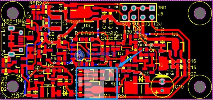
High-Speed Universal Serial Bus (USB) technology has become a ubiquitous standard in modern electronic devices, offering fast data transfer rates and versatile connectivity options. Designing a printed circuit board (PCB) that incorporates high-speed USB interfaces requires careful consideration of signal integrity, power delivery, and electromagnetic compatibility (EMC). This article provides essential guidelines and best practices to ensure successful high-speed USB PCB layout design, which is crucial for achieving optimal performance and reliability.
USB High-Speed supports data rates up to 480 Mbps. It uses differential signaling over twisted-pair cables or traces on the PCB. Familiarity with USB specifications, including pinouts, signal characteristics, and electrical requirements, is fundamental. Compliance with the USB 2.0 High-Speed Electrical Specification ensures interoperability and minimizes errors during high-speed data transmission.

Trace Length Matching:
For the D+ and D- differential pair signals, strive to maintain matched trace lengths to within ±50 mils to minimize skew and intersymbol interference (ISI). Use a serpentine pattern if necessary to match lengths without affecting the overall route length significantly.
Trace Impedance Control:
Controlled impedance routing is critical for high-speed USB signals. The typical target impedance is 90 ohms differential and 45 ohms single-ended. Ensure that your PCB stackup allows for precise control of trace impedance throughout the layout.
Proximity and Separation:
Keep the differential pair tightly coupled with a consistent spacing throughout their length to maintain good common mode rejection. Separate the differential pair from other high-speed signals, power planes, and ground planes by at least 3H (where H is the height of the dielectric layer).
Decoupling Capacitors:
Place decoupling capacitors (0.1 uF ceramic) as close as possible to the USB transceiver's VCC pins, ideally within a few millimeters. Additionally, use bulk capacitance for stability.
Ground Planes:
A solid ground plane beneath the USB signals helps reduce noise and maintains a low-impedance return path. Ensure that the ground plane under the USB traces is continuous and not interrupted by vias or splits.
Series Termination Resistors:
Include series termination resistors at the end of each USB signal line to match the characteristic impedance of the cable and PCB traces. This reduces signal reflections and improves signal quality.
ESD Protection Components:
Protect the USB interface with suitable ESD protection diodes or TVS diodes to safeguard against electrostatic discharge events.
Position the USB connector such that the signal traces have the shortest possible path to the transceiver. Orient the connector so that the signal pairs run parallel to the edge of the PCB to limit stubs and improve signal integrity.
Before finalizing the layout, perform signal integrity simulations to verify crosstalk, impedance control, and potential issues related to reflections and ringing. This step is vital in ensuring the USB interface meets the required performance standards.
After fabrication, validate the PCB design through compliance testing. This includes tests like eye diagram analysis, link training, and signal quality measurements to confirm adherence to USB high-speed specifications.
Designing a high-speed USB interface on a PCB demands meticulous attention to detail in terms of routing, component placement, and signal integrity measures. Adhering to these layout recommendations will not only enhance the performance of your USB interface but also contribute to its long-term reliability and compatibility across various systems. By following industry-standard practices and utilizing advanced design tools, engineers can confidently implement high-speed USB interfaces in their designs while mitigating potential issues associated with high-frequency signal transmission.
1:How do I choose the right USB connector type for my high-speed application?
When selecting a USB connector, consider factors such as the required data rate (USB 2.0 High-Speed vs. USB 3.x SuperSpeed), mechanical durability, and environmental conditions. Type-A, B, micro-B, and USB-C connectors all support high-speed operation, but USB-C is preferred for newer designs due to its reversible nature and higher speed capabilities (up to 10 Gbps for USB 3.2 Gen 2). Always choose connectors that are certified for the specific USB version you're working with to ensure compatibility and reliable performance.
2.How important is it to adhere to the USB 2.0 High-Speed cable assembly specifications when designing the PCB?
Adhering to cable assembly specifications is crucial because the PCB layout should be compatible with the expected cable characteristics. This involves considering the cable's characteristic impedance, attenuation, and skew, which can affect signal integrity when transitioning from the PCB to the cable. If the PCB does not account for these variables, it could lead to signal degradation, data errors, or even failure to establish a connection.
3:What are some tips for managing crosstalk between high-speed USB signals and other components on the PCB?
To minimize crosstalk:
- Route high-speed USB signals away from sensitive analog circuits and clock lines.
- Maintain sufficient clearance between adjacent traces.
- Use shielding techniques like guard traces or ground pours around sensitive areas.
- Implement strategic via stitching to create a continuous ground plane and minimize loop areas.
- Apply proper layer stack-up design to lower coupling capacitance between signal layers.
4: Can thermal considerations impact high-speed USB PCB layout?
Yes, thermal management is an essential aspect of any PCB design, including those with high-speed USB interfaces. High currents flowing through the VBUS line can generate heat, which might affect nearby components or degrade signal quality. Therefore, ensure adequate copper pour for VBUS traces and use thermal vias to dissipate heat effectively. Moreover, avoid placing temperature-sensitive components near power-hungry elements like USB transceivers.
5.Are there any specific software tools that can assist with high-speed USB PCB layout optimization?
Several PCB design software packages include features specifically designed for high-speed digital designs, such as Altium Designer, Cadence Allegro, Mentor Graphics Xpedition, and Zuken CR-8000. These tools offer simulation capabilities for signal integrity, power integrity, and EMC analysis. They help designers predict and mitigate issues before fabrication, making them indispensable for creating robust high-speed USB interfaces.