Professional China PCB Assembly Online Services
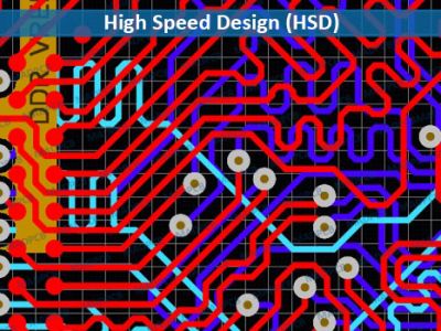
Printed circuit boards (PCBs) are the backbone of modern electronics, enabling complex circuits and components to be integrated into compact and reliable devices. However, as the demand for faster, smaller, and more powerful electronics increases, PCB designers face new challenges in ensuring the performance and integrity of their designs. High-speed PCB design is a specialized field that requires careful attention to various factors such as signal propagation, electromagnetic interference (EMI), power integrity, thermal management, and more. In this article, we will explore some of the key aspects of high-speed PCB design, including the principles, materials, layout, and stackup techniques that can help you achieve optimal results.
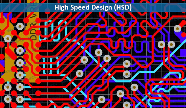
Before diving into the details of high-speed PCB design, it is important to understand what makes a PCB high-speed in the first place. There is no definitive answer to this question, as different applications may have different criteria for defining high-speed. However, a general rule of thumb is that a PCB can be considered high-speed if the signal rise or fall time is less than or equal to one-sixth of the signal propagation delay across the board. This means that the signal transitions from low to high or vice versa faster than it travels from one end of the board to the other. In other words, the signal behaves more like a wave than a voltage level.
When dealing with high-speed signals, PCB designers need to consider several factors that can affect the signal quality and performance, such as:
- Impedance: The opposition to the flow of current in an AC circuit, which depends on the frequency, geometry, and material properties of the circuit. Impedance mismatch can cause signal reflections, distortions, and losses.
- Crosstalk: The unwanted coupling of signals between adjacent traces or layers, which can cause interference, noise, and reduced signal-to-noise ratio (SNR).
- EMI: The generation or reception of electromagnetic radiation by electrical circuits or components, which can cause interference with other devices or systems.
- Power integrity: The ability to deliver stable and clean power to all components on the board, which can affect the performance, reliability, and efficiency of the circuit.
- Thermal management: The dissipation of heat generated by electrical components or traces, which can affect the functionality, lifespan, and safety of the circuit.
To address these challenges, high-speed PCB designers need to follow some basic principles such as:
- Matching impedance between drivers, receivers, and transmission lines to minimize reflections and losses.
- Minimizing trace lengths and bends to reduce signal delay and attenuation.
- Separating analog and digital signals to avoid crosstalk and interference.
- Using proper grounding techniques to provide a low-impedance return path for signals and reduce noise.
- Applying decoupling capacitors and bypass filters to smooth out voltage fluctuations and noise on power rails.
- Using adequate cooling methods such as heatsinks, fans, or thermal vias to dissipate heat from hot spots.
Another crucial aspect of high-speed PCB design is choosing the right materials for the board. The choice of materials can have a significant impact on the electrical characteristics of the board, such as dielectric constant (Dk), dielectric loss tangent (Df), coefficient of thermal expansion (CTE), thermal conductivity (k), and more. These parameters affect how signals propagate through the board, how much energy is lost or dissipated along the way, how much the board expands or contracts due to temperature changes, and how well it conducts heat.
Some of the common materials used for high-speed PCBs are:
- FR-4: The most widely used material for general-purpose PCBs. It is a composite of glass fiber and epoxy resin with a Dk of about 4.5 and a Df of about 0.02 at 1 GHz. It has good mechanical strength and dimensional stability but relatively high dielectric loss and moisture absorption.
- Polyimide: A high-performance material with excellent thermal stability and resistance to chemicals and radiation. It has a Dk of about 3.5 and a Df of about 0.003 at 1 GHz. It has low dielectric loss but high cost and brittleness.
- PTFE: A synthetic polymer with very low dielectric loss and high resistance to heat and chemicals. It has a Dk of about 2.1 and a Df of about 0.0002 at 1 GHz. It has low dielectric constant but high CTE and low adhesion to copper.
- Ceramic: A material with very high thermal conductivity and low CTE. It has a Dk of about 9.8 and a Df of about 0.001 at 1 GHz. It has high dielectric constant but high cost and fragility.
The choice of material depends on the specific requirements and trade-offs of the application. For example, FR-4 may be suitable for low to medium speed applications, while polyimide or PTFE may be preferred for high-speed or high-frequency applications. Ceramic may be ideal for applications that require high thermal performance or low noise.
Once the materials are selected, the next step is to design the layout of the board. The layout is the physical arrangement of the components and traces on the board, which determines how signals flow and interact with each other. A good layout can enhance the performance and reliability of the board, while a bad layout can degrade or even ruin it.
Some of the essential guidelines for high-speed PCB layout are:
- Use differential signaling whenever possible. Differential signaling is a technique that uses two complementary signals to transmit data, such as +V and -V. This reduces the susceptibility to noise and crosstalk, as any common-mode noise or interference will cancel out in the receiver. Differential signaling also allows higher data rates and lower voltage levels, which reduces power consumption and EMI.
- Route critical signals first. Critical signals are those that have the highest speed, frequency, or sensitivity, such as clock signals, data buses, or analog signals. These signals should be routed first to ensure they have the shortest and most direct paths, with minimal vias, bends, or stubs. This reduces signal delay, distortion, and loss, as well as crosstalk and EMI.
- Use controlled impedance routing. Controlled impedance routing is a technique that ensures that the impedance of the traces matches the impedance of the drivers and receivers, as well as the impedance of the transmission lines. This minimizes signal reflections and losses, which can degrade signal quality and cause errors or failures. Controlled impedance routing requires careful calculation of trace width, spacing, thickness, and dielectric properties, as well as verification using impedance testing equipment.
- Avoid parallel routing of adjacent traces or layers. Parallel routing of adjacent traces or layers can cause crosstalk and interference, as signals can couple capacitively or inductively between them. This can reduce signal-to-noise ratio (SNR) and cause errors or failures. To avoid parallel routing, use orthogonal routing (perpendicular or 45-degree angles) between adjacent traces or layers, or use shielding techniques such as guard traces or ground planes.
- Use proper termination techniques. Termination is a technique that adds resistors or other components at the end of a transmission line to match its impedance and absorb any reflected signals. This prevents signal reflections from traveling back and forth along the line, which can cause signal degradation and interference. Termination techniques include series termination, parallel termination, Thevenin termination, AC termination, and more.
In addition to the essential guidelines for high-speed PCB layout, there are some best practices that can further improve the performance and reliability of the board. These best practices include:
- Use a multilayer board design. A multilayer board design is a design that uses more than two layers of copper and dielectric to create a PCB. A multilayer board design offers several advantages for high-speed PCB design, such as:
- More routing space and flexibility
- Better signal integrity and isolation
- Lower parasitic capacitance and inductance
- Better power distribution and integrity
- Better thermal management and dissipation
However, a multilayer board design also has some disadvantages, such as:
- Higher cost and complexity
- More difficult fabrication and testing
- Higher risk of manufacturing defects
Therefore, a multilayer board design should be used only when necessary and optimized for the specific application.
- Use a proper power distribution network (PDN). A PDN is a network of power sources, traces, planes, vias, capacitors, filters, regulators, and loads that delivers power to all components on the board. A proper PDN ensures that all components receive stable and clean power with minimal voltage drops or fluctuations. This improves the performance, reliability, and efficiency of the circuit.
Some of the key aspects of designing a proper PDN are:
- Use a dedicated power plane for each voltage level
- Use thick traces or planes to reduce resistance and voltage drops
- Use multiple vias to connect power planes to reduce inductance
- Use decoupling capacitors near each component to smooth out voltage fluctuations
- Use bypass filters to filter out high-frequency noise from power sources
- Use voltage regulators to convert or regulate voltage levels
- Use proper grounding techniques. Grounding is a technique that connects all components on the board to a common reference point or potential, usually zero volts. Grounding provides a low-impedance return path for signals and currents, as well as a shield against noise and interference.
Some of the key aspects of designing a proper grounding system are:
- The type and location of the grounding electrodes. The grounding electrodes are the conductive elements that connect the electrical system to the earth. They can be rods, plates, wires, pipes, or other metallic objects that are buried in the soil or submerged in water. The type and location of the grounding electrodes depend on the soil resistivity, the fault current magnitude, the environmental conditions, and the availability of space.
- The size and material of the grounding conductors. The grounding conductors are the wires or cables that connect the grounding electrodes to the electrical equipment or devices that need to be grounded. The size and material of the grounding conductors depend on the current carrying capacity, the voltage drop, the corrosion resistance, and the mechanical strength.
- The configuration and layout of the grounding system. The configuration and layout of the grounding system refer to how the grounding electrodes and conductors are arranged and connected to form a low impedance path for fault currents to flow to the earth. The configuration and layout of the grounding system depend on the type and number of electrical sources, loads, and circuits, as well as the safety and performance requirements.
- The testing and maintenance of the grounding system. The testing and maintenance of the grounding system are essential to ensure that it is functioning properly and meets the standards and codes. The testing and maintenance of the grounding system include measuring the resistance, continuity, and potential of the grounding electrodes and conductors, inspecting for physical damage or deterioration, and repairing or replacing any defective components.