Professional China PCB Assembly Online Services

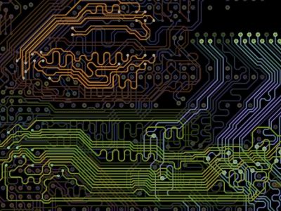
Designing a high-speed PCB requires careful consideration of several key factors to ensure optimal performance and reliability. Here are some essential considerations:
1. Signal Integrity:
Maintain signal integrity to minimize signal degradation and ensure proper data transmission.
Address issues such as reflections, ringing, and overshoot/undershoot.
2. Impedance Matching:
Achieve controlled impedance for transmission lines to prevent signal reflections and maintain signal integrity.
Use impedance matching techniques for connectors, vias, and traces.
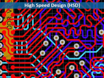
3. Routing and Trace Length Matching:
Pay attention to the routing of high-speed signals, keeping trace lengths matched to control skew and timing issues.
Minimize signal path length to reduce signal propagation delay.
4. Grounding and Return Paths:
Design a solid ground plane to provide a low-impedance return path for signals.
Minimize ground loops and ensure proper grounding techniques to avoid noise.
5. Power Distribution:
Implement a robust power distribution network to provide stable and clean power to components.
Use decoupling capacitors strategically to manage power fluctuations.
6. EMI and EMC Considerations:
Employ techniques to minimize electromagnetic interference (EMI) to prevent signal degradation and interference with other components.
Ensure compliance with electromagnetic compatibility (EMC) standards.
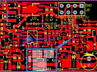
7. Component Placement:
Carefully place components to minimize trace lengths and reduce parasitic capacitance and inductance.
Group components logically based on their function to optimize signal paths.
8. Material Selection:
Choose appropriate PCB materials based on dielectric constants, thermal properties, and signal speed requirements.
Consider the impact of material properties on signal integrity and loss.
9. Thermal Management:
Address heat dissipation issues to prevent overheating of components.
Ensure proper ventilation and consider the use of heat sinks or thermal vias.
10. Differential Pair Routing:
Implement proper routing techniques for differential pairs to maintain signal balance and minimize common-mode noise.
Control the spacing and impedance of differential traces.
11. Testing and Validation:
Perform thorough signal integrity simulations and analyses.
Conduct testing, including eye diagram analysis, bit error rate (BER) testing, and compliance testing.
12. Future Scalability:
Design the PCB with future upgrades and scalability in mind.
Consider potential changes in technology and standards.
By addressing these key factors, designers can create high-speed PCBs that meet performance requirements and ensure the reliability of electronic systems.