Professional China PCB Assembly Online Services
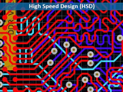
In the rapidly evolving landscape of electronics, the demand for high-speed pcb has become paramount. This article aims to demystify the intricacies of high-speed PCB design, providing a comprehensive guide for engineers and enthusiasts alike. As we delve into the nuances of this specialized field, we'll explore the profound impact that high-speed PCB design has on advanced electronics manufacturing.
Section 1: Understanding High-Speed PCB Design :
What is High-Speed PCB Design?
High-Speed PCB Design refers to the specialized process of creating printed circuit boards (PCBs) that are engineered to operate at elevated frequencies, typically in the gigahertz (GHz) range. This discipline is crucial in the design and development of electronic systems where signal integrity, timing, and data transfer rates are of paramount importance. The goal of high-speed PCB design is to ensure that signals can propagate across the circuit board with minimal distortion, noise, and attenuation.
Key Aspects of High-Speed PCB Design:
Power Integrity:
Ensuring a stable and clean power supply is essential. High-speed components often have stringent power delivery network requirements to minimize voltage fluctuations.
EMI/EMC Considerations:
Electromagnetic Interference (EMI) and Electromagnetic Compatibility (EMC) are critical in high-speed designs. Proper shielding and layout practices help mitigate interference and ensure compliance with regulatory standards.
Component Placement:
Careful placement of components is vital to minimize signal travel distances, reduce parasitic capacitance and inductance, and optimize the overall signal path.
Grounding Strategies:
Establishing effective grounding strategies is crucial for high-speed designs. A well-designed ground plane helps in minimizing ground loops and ensures a low-impedance return path for signals.
Materials and Substrates:
The choice of materials and substrates for the PCB is important. High-quality dielectric materials with specific characteristics are selected to meet the requirements of high-speed signals.
Simulation and Analysis:
Utilizing simulation tools to model and analyze the behavior of high-speed signals helps designers predict and address potential issues before the PCB is manufactured.
Compliance with Standards:
Adhering to industry standards and specifications is essential for ensuring compatibility, reliability, and interoperability of high-speed electronic systems.
High-speed PCB design is a multidisciplinary field that requires a deep understanding of electrical engineering, electromagnetic theory, and practical design considerations. Engineers specializing in this area play a crucial role in the development of cutting-edge technologies, such as high-performance computing, telecommunications, and advanced electronic devices.

Section 2: An Introduction to High-Speed Printed Circuit Boards
In the ever-evolving landscape of electronics, the demand for faster and more efficient electronic systems has given rise to the importance of High-Speed Printed Circuit Boards (PCBs). These specialized PCBs play a crucial role in facilitating the rapid transmission of signals, enabling the seamless operation of advanced electronic devices. This introduction serves as a primer on High-Speed Printed Circuit Boards, shedding light on their significance, key characteristics, and the challenges involved in their design and implementation.
Defining High-Speed Printed Circuit Boards:
High-Speed Printed Circuit Boards, often abbreviated as high-speed PCBs, are designed to accommodate signals that operate at frequencies beyond the range of traditional circuit boards. These frequencies typically extend into the gigahertz (GHz) range, necessitating meticulous design considerations to maintain signal integrity and minimize transmission delays.
Key Characteristics:
Signal Frequencies:
High-speed PCBs are characterized by their ability to handle signals with frequencies in the GHz range. This includes applications in fields such as telecommunications, data communications, and high-performance computing.
Signal Integrity:
Maintaining the integrity of signals is paramount. High-speed PCB design addresses challenges like signal distortion, crosstalk, and impedance matching to ensure accurate and reliable signal transmission.
Impedance Control:
Precise control of impedance throughout the PCB is crucial. This involves maintaining consistent impedance along transmission lines to prevent signal reflections and distortions.
Layout and Routing:
The layout and routing of traces on high-speed PCBs are optimized to minimize signal travel distances, reduce parasitic effects, and ensure efficient signal propagation.
Materials and Substrates:
High-quality materials and substrates are chosen to meet the specific requirements of high-speed signals. Dielectric materials with low loss and controlled characteristics are often employed.
Component Placement:
Strategic placement of components is essential to minimize signal path lengths, reduce interference, and optimize the overall performance of the high-speed PCB.
Power Distribution:
Ensuring stable power distribution is critical. High-speed components often have stringent power delivery network requirements to minimize voltage fluctuations and ensure reliable operation.
EMI/EMC Considerations:
Electromagnetic Interference (EMI) and Electromagnetic Compatibility (EMC) are carefully addressed to meet regulatory standards and ensure the reliable operation of electronic systems in complex environments.
Challenges in High-Speed PCB Design:
Designing high-speed PCBs presents unique challenges, including signal integrity issues, thermal management, and the need for advanced simulation and analysis tools. Engineers specializing in high-speed PCB design must navigate these challenges to deliver electronic systems that meet the growing demands for speed, efficiency, and reliability.
Conclusion:
As technology continues to advance, the role of High-Speed Printed Circuit Boards becomes increasingly critical in shaping the capabilities of electronic devices. This introduction provides a glimpse into the world of high-speed PCBs, setting the stage for a deeper exploration of the principles, guidelines, and innovations that drive this dynamic field of electronic design.

Section 3: High-Speed PCB Design Guidelines You Must Know
High-speed printed circuit board (PCB) design is a specialized field that demands precision, attention to detail, and a deep understanding of the unique challenges posed by high-frequency signals. To ensure optimal performance and reliability in electronic systems operating at elevated speeds, engineers must adhere to specific guidelines throughout the design process. Here are essential high-speed PCB design guidelines that every designer must be well-acquainted with:
Impedance Matching:
Maintain consistent impedance across transmission lines to prevent signal reflections and ensure signal integrity. Use controlled impedance traces and consider the impedance of connectors and components.
Signal Integrity Analysis:
Employ simulation tools to analyze and optimize signal integrity. This includes assessing signal rise times, eye diagrams, and identifying potential signal integrity issues early in the design phase.
Ground Plane Design:
Establish a solid ground plane to provide a low-impedance return path for signals. Proper grounding minimizes noise, reduces electromagnetic interference (EMI), and enhances the overall performance of the PCB.
Decoupling Capacitors:
Place decoupling capacitors strategically near high-speed components to stabilize the power supply and minimize voltage fluctuations. This is crucial for preventing noise and ensuring proper functionality.
Trace Routing:
Pay careful attention to trace routing. Minimize trace lengths, avoid sharp angles, and use controlled impedance routing for critical signals. Differential pairs should be routed closely together to maintain signal integrity.
Crosstalk Mitigation:
Prevent crosstalk between adjacent traces by maintaining appropriate spacing and using shielding techniques. Differential signaling and staggered trace arrangements can help minimize the impact of crosstalk.Power Distribution Network (PDN):
Design an efficient power distribution network to ensure stable and clean power delivery to all components. Properly manage power planes and use low-inductance power distribution to minimize voltage drops.
Thermal Management:
High-speed components generate heat, and effective thermal management is crucial for preventing overheating. Consider the placement of heat sinks, thermal vias, and ensure adequate ventilation in the overall system.
Component Placement:
Strategically place components to minimize signal path lengths and reduce parasitic capacitance and inductance. Group components according to their functionalities and thermal considerations.
Backdrilling for Vias:
Implement backdrilling for vias to reduce signal reflections caused by excess stub length. Backdrilling helps maintain signal integrity and is particularly important for high-speed designs.
EMI Shielding:
Incorporate electromagnetic interference (EMI) shielding techniques to minimize the impact of external electromagnetic fields on the PCB. Shield critical components and sensitive traces to ensure reliable operation.
Documentation and Collaboration:
Maintain comprehensive documentation throughout the design process. Clear and accurate documentation aids in collaboration, troubleshooting, and future modifications.
By adhering to these high-speed PCB design guidelines, engineers can navigate the complexities of designing circuits that operate at elevated frequencies. These principles not only enhance the performance and reliability of high-speed electronic systems but also contribute to the overall success of advanced technologies in diverse applications.

Section 4: The Effect of High-Speed PCB Design in Advanced Electronics Manufacturing
As the demand for faster and more sophisticated electronic devices continues to rise, the impact of high-speed printed circuit board (PCB) design on advanced electronics manufacturing becomes increasingly profound. This article explores the multifaceted effects of high-speed PCB design on the manufacturing processes and the overall landscape of advanced electronics.
Performance Enhancement:
High-speed PCB design directly contributes to the improved performance of electronic devices. By optimizing signal paths, minimizing signal distortions, and ensuring signal integrity, high-speed PCBs enable faster data transfer rates and enhanced overall system responsiveness.
Reduced Latency:
In applications such as telecommunications, high-performance computing, and data centers, reduced latency is a critical factor. High-speed PCB design facilitates the swift transmission of signals, leading to minimized delays and improved real-time processing capabilities.
Miniaturization and Component Density:
High-speed PCBs often involve intricate designs that allow for compact layouts and increased component density. This miniaturization is crucial for advanced electronics manufacturing, enabling the creation of smaller, lighter, and more powerful electronic devices.
Energy Efficiency:
The efficient design of high-speed PCBs contributes to energy efficiency in electronic systems. By optimizing signal paths and power distribution networks, high-speed PCBs help reduce power consumption and contribute to the development of energy-efficient devices.
Reliability and Robustness:
Rigorous adherence to high-speed PCB design principles enhances the reliability and robustness of electronic systems. The mitigation of signal integrity issues, proper thermal management, and adherence to industry standards result in electronic devices that operate consistently and withstand challenging environmental conditions.
Manufacturability Challenges:
The complexity of high-speed PCBs introduces challenges in the manufacturing process. Advanced manufacturing techniques, precision equipment, and stringent quality control measures become imperative to ensure the successful fabrication of high-speed PCBs.
Advanced Materials and Manufacturing Technologies:
High-speed PCB design often necessitates the use of advanced materials with specific electrical and thermal characteristics. Additionally, manufacturing technologies such as laser drilling, high-precision etching, and controlled impedance testing become integral to producing high-quality, high-speed PCBs.
Cost Considerations:
While high-speed PCBs offer unparalleled performance benefits, there are associated costs related to advanced materials, manufacturing processes, and quality control. Balancing performance improvements with cost considerations is crucial in the production of high-speed electronic devices.
Cross-Disciplinary Collaboration:
High-speed PCB design requires collaboration among electrical engineers, mechanical engineers, and manufacturing specialists. Effective communication and interdisciplinary collaboration are essential for overcoming challenges and optimizing the overall manufacturing process.
Impact on Emerging Technologies:
High-speed PCB design plays a pivotal role in shaping emerging technologies such as 5G communications, artificial intelligence, and the Internet of Things (IoT). The capabilities of these technologies are often dependent on the efficiency and speed of the underlying electronic systems.
In conclusion, the effect of high-speed PCB design in advanced electronics manufacturing is transformative. From enhancing performance and reducing latency to enabling miniaturization and improving energy efficiency, high-speed PCBs are instrumental in driving innovation in the realm of advanced electronics. As manufacturing techniques continue to evolve, high-speed PCB design will remain a cornerstone in the development of cutting-edge electronic devices that define the future of technology.