Professional China PCB Assembly Online Services
Custom Printed Circuit Board (PCB) design is a crucial aspect of electronic product development, facilitating the translation of circuit schematics into physical boards that power a wide array of devices. The process begins with the definition of project requirements, where specifications such as functionality, size, and power consumption are outlined. Following this, engineers create a schematic diagram detailing the interconnections of components, after which suitable components are selected based on technical requirements and cost considerations. This initial phase sets the foundation for the subsequent steps in the custom PCB design process, leading to the creation of a bespoke PCB that aligns with the unique needs of the electronic system being developed.
Here is an overview of the typical process:
1.Define Requirements:
Clearly define the specifications and requirements of your electronic device or system.
Determine the functionality, size, power requirements, and other key parameters.
2.Schematic Design:
Create a schematic diagram that illustrates the components in your circuit and their connections.
Choose appropriate components and ensure compatibility.
3.Component Selection:
Choose components based on the schematic design, considering factors like availability, cost, and technical specifications.
Create a bill of materials (BOM) listing all components.
4.Create Footprints:
Develop footprints for each component to represent its physical layout on the PCB.
Footprints define the pad locations and other features necessary for component placement.
5.PCB Layout Design:
Use a PCB design software to place components on the board and route the connections.
Consider factors like signal integrity, power distribution, and thermal management during layout.
6.Routing:
Route traces to connect the pads of components, ensuring proper signal integrity and avoiding interference.
Follow best practices for signal routing, such as minimizing trace lengths and avoiding signal crosstalk.
7.Design Rule Check (DRC):
Run a Design Rule Check to ensure that your layout complies with the manufacturing capabilities of your chosen PCB fabrication service.
Fix any errors or violations identified by the DRC.
8.Gerber File Generation:
Generate Gerber files, which are standard files used by PCB manufacturers to create the physical PCB.
Gerber files include information about copper layers, solder mask, silkscreen, and other details.
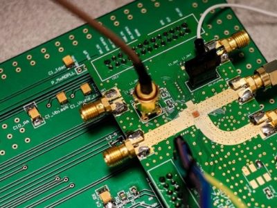
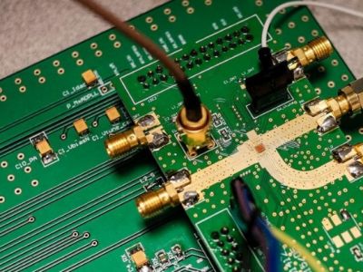
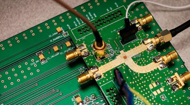
9.Prototype Fabrication:
Send the Gerber files to a PCB fabrication house to produce a prototype of your custom PCB.
Verify the functionality of the prototype to ensure it meets design specifications.
10.Testing and Debugging:
Test the prototype to identify and address any issues or bugs.
Use tools like oscilloscopes, multimeters, and logic analyzers for debugging.
1.Optimization and Iteration:
Make any necessary adjustments to the design based on testing results.
Optimize the layout for performance, cost, and manufacturability.
Iterate the design if needed and go through additional prototyping and testing cycles.
2.Documentation:
Create comprehensive documentation, including schematics, PCB layout files, BOM, assembly instructions, and testing procedures.
This documentation is crucial for future revisions, troubleshooting, and mass production.
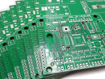
3.Mass Production:
Once the design is finalized and thoroughly tested, send the final design files to a PCB manufacturer for mass production.
Throughout the custom PCB design process, collaboration between electrical engineers, PCB designers, and manufacturers is essential to ensure a successful outcome.