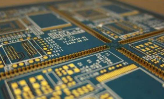
A multilayer PCB stackup refers to the arrangement and organization of different layers in a multilayer printed circuit board (PCB). It defines the sequence, thickness, and materials of each layer, as well as the interconnections between them. The stackup plays a crucial role in determining the electrical performance, signal integrity, and overall functionality of the PCB.
Signal Layers: These layers carry electrical signals between components on the PCB. They typically consist of copper traces and are separated by dielectric materials.
Power and Ground Planes: Power and ground planes provide stable voltage and reference points for the electronic components on the PCB. They are usually solid copper layers.
Dielectric Layers: Dielectric materials, such as fiberglass or prepreg, are used to insulate and separate the conductive layers in the PCB.
Core and Prepreg: The core is a thin sheet of dielectric material with copper cladding on one or both sides. Prepreg is a resin-coated dielectric material used to bond the core layers together.
Symmetrical Stackup: In a symmetrical stackup, the signal layers are evenly distributed between the power and ground planes. This type of stackup provides good signal integrity and controlled impedance.
Asymmetrical Stackup: Asymmetrical stackups have an uneven distribution of signal layers relative to the power and ground planes. This type of stackup is often used to optimize signal routing and accommodate specific design requirements.
Signal Integrity: The stackup should be designed to minimize signal loss, crosstalk, and impedance mismatch to ensure reliable signal transmission.
Power Distribution: The stackup should provide adequate power and ground distribution to all components on the PCB, avoiding voltage drops and noise issues.
Thermal Management: The stackup should consider heat dissipation requirements to prevent overheating and ensure the proper functioning of the PCB.
EMI/RFI Control: The stackup should incorporate shielding layers or other techniques to minimize electromagnetic interference (EMI) and radio frequency interference (RFI).
Compact Size: Multilayer PCBs allow for the integration of multiple circuits in a single board, reducing the overall size and weight of the electronic device.
Improved Performance: Multilayer PCBs enable better signal integrity, controlled impedance, and reduced noise, leading to improved electrical performance.
Design Flexibility: Multilayer PCBs provide greater design flexibility, allowing for complex routing and the accommodation of a wide range of components.
Reliability: Multilayer PCBs are generally more reliable due to their robust construction and reduced risk of manufacturing defects.
Creating a multilayer PCB stackup involves determining the number and arrangement of layers in your design, including signal layers, power and ground planes, and any additional internal layers. Here's a step-by-step guide to help you create a multilayer PCB stackup:

Determine the Number of Layers: Understand the complexity and requirements of your circuit design to determine the number of layers needed in your PCB stackup. This decision depends on factors such as signal density, component count, and the need for power and ground planes.
Layer Ordering: Decide the order in which you'll stack the layers. Typically, a multilayer PCB stackup starts with a signal layer, followed by alternating power and ground planes, and ends with another signal layer. The outer layers are often signal layers, while inner layers are dedicated to power and ground planes.
Signal Layers: Determine the number of signal layers required based on the complexity of your design and the number of signal traces. Signal layers carry the actual circuitry and should be placed between the power and ground planes to minimize noise and interference.
Power and Ground Planes: Allocate power and ground planes in your PCB stackup. Power planes provide a stable voltage reference and distribute power to the components, while ground planes serve as a low impedance return path for signals and help reduce noise.
Additional Internal Layers: Depending on the complexity of your design, you may need additional internal layers for specific purposes. These layers can be used for routing high-speed signals, implementing differential pairs, creating impedance-controlled traces, or accommodating special requirements like RF shielding.
Layer Ordering and Spacing: Determine the order of the layers in your stackup and the spacing between them. Typically, a common order is (from top to bottom): signal layer, prepreg (insulating material), power plane, core (dielectric material), ground plane, and prepreg.
Dielectric Material Selection: Choose the appropriate dielectric material for the core and prepreg layers in your stackup. Consider factors such as dielectric constant (Dk), dissipation factor (Df), glass transition temperature (Tg), and the required thickness to meet the electrical and mechanical specifications of your design.
Layer Thickness: Determine the thickness of each layer in your stackup. The layer thickness is crucial for controlling impedance, minimizing crosstalk, and meeting mechanical requirements. Consider the specifications of the chosen dielectric material and consult PCB design guidelines for recommended layer thicknesses.
Controlled Impedance: If your design includes high-speed signals or impedance-controlled traces, ensure that the layer stackup is designed to maintain consistent impedance values. This may involve specifying specific layer thicknesses and dielectric materials to achieve the desired impedance characteristics.
Document the Stackup: Create a detailed documentation of the PCB stackup, including the number of layers, layer ordering, layer thicknesses, dielectric materials used, and any other specifications relevant to your design. This documentation will serve as a reference during the PCB fabrication process.
Remember, the specific requirements of your design and the manufacturing capabilities of your chosen PCB manufacturer will influence your stackup decisions. It's important to consult the manufacturer's guidelines and seek expert advice.
Multilayer PCB stackup design is a critical aspect of PCB manufacturing, influencing the board's performance, functionality, and reliability. By carefully considering factors such as signal integrity, power distribution, thermal management, and EMI/RFI control, designers can optimize the stackup to meet the specific requirements of their electronic device. As technology continues to advance, multilayer PCBs with complex stackups will play a vital role in enabling the development of high-speed, high-density electronic systems.
Get more knowledge about Multilayer PCB Stackup please refer to Rigaopcb:https://www.rigaopcb.com/