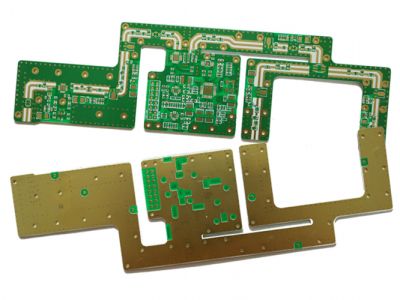
Professional China PCB Assembly Online Services
In the dynamic realm of electronics manufacturing, the relentless pursuit of speed, efficiency, and reliability propels the industry forward. At the heart of this evolution lies the intricate world of High-Frequency PCBs (HF PCBs), a critical element that enables the transmission of signals at frequencies beyond the scope of traditional printed circuit boards. As the demand for faster and more sophisticated electronic devices intensifies, mastering the intricacies of High-Frequency PCB design becomes a cornerstone for engineers and designers.

This article embarks on a comprehensive exploration of High-Frequency PCBs, traversing through their fundamental significance, the nuances of their design, layout optimization strategies, meticulous material selection, and the implementation of best practices. By unraveling the complexities surrounding HF PCBs, this discussion aims to empower electronics professionals with the knowledge and insights needed to navigate the challenges of designing and manufacturing cutting-edge electronic devices.
Let's delve into the core components of mastering High-Frequency PCB design, where understanding, optimizing, and implementing best practices converge to unlock the full potential of electronics manufacturing in the high-frequency spectrum.
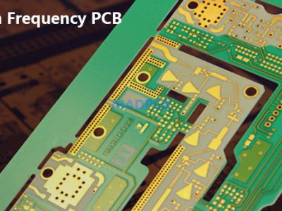
What is High Frequency (HF) PCB?
High Frequency (HF) PCB refers to a type of printed circuit board designed to operate at radio frequencies (RF) or microwave frequencies. These frequencies typically range from 3 megahertz (MHz) to 300 gigahertz (GHz) or even higher. HF PCBs are commonly used in applications such as wireless communication systems, radar systems, satellite communication, and high-speed digital data transfer.
The design and manufacturing of HF PCBs involve several considerations to ensure optimal performance at high frequencies:
1.Material Selection:
The choice of substrate material is crucial for HF PCBs. Materials with low dielectric constants, such as PTFE (Polytetrafluoroethylene) or FR-4 with a high-frequency grade, are often preferred because they minimize signal loss and maintain signal integrity.
2.Impedance Control:
Maintaining consistent impedance is vital for high-frequency signals to prevent signal reflections and ensure proper signal transmission. Designers use controlled impedance traces and careful routing techniques to achieve this.
3.Signal Integrity:
HF PCBs require careful consideration of signal integrity to minimize signal distortion, crosstalk, and electromagnetic interference (EMI). This involves proper ground plane design, controlled impedance, and signal trace routing.
4.Copper Thickness
The thickness of the copper traces on the PCB affects its performance at high frequencies. Thicker copper can provide better conductivity and lower impedance but may also lead to increased signal loss.
5.Via Design:
Vias play a critical role in connecting different layers of the PCB. In HF PCBs, it's important to minimize the impact of vias on signal integrity by using proper via designs and minimizing the number of vias.
6.Shielding:
To minimize electromagnetic interference and maintain signal integrity, HF PCBs may incorporate shielding techniques. This can involve adding ground planes or employing shielding cans around sensitive components.
7.Surface Finish:
The choice of surface finish is important for HF PCBs. Immersion gold (ENIG) or immersion silver are often preferred due to their smooth surfaces and good conductivity.
HF PCBs are essential for applications where precise signal transmission and reception are critical. Designing and manufacturing these boards require specialized knowledge and attention to detail to ensure optimal performance in high-frequency environments.

Designing High-Frequency PCBs
Designing high-frequency PCBs requires careful consideration of various factors to ensure optimal performance at radio frequencies (RF) or microwave frequencies. Here are some key aspects to focus on when designing high-frequency PCBs:
1.Substrate Material Selection:
Choose a substrate material with a low dielectric constant (εr) to minimize signal loss. Materials like PTFE (Teflon) or high-frequency grade FR-4 are commonly used.
Consider the thermal and mechanical properties of the substrate material to ensure stability at high frequencies.
2.Impedance Matching and Control:
Maintain controlled impedance throughout the PCB design to prevent signal reflections and ensure efficient signal transmission.
Use impedance calculation tools and simulation software to determine trace widths and dielectric thickness for the desired impedance.
3.Signal Integrity:
Minimize signal distortion, crosstalk, and EMI by carefully designing the signal traces, ground planes, and power distribution.
Keep signal traces short and direct to reduce signal propagation delays.
4.Grounding and Power Distribution:
Implement a solid ground plane to provide a low-impedance return path for signals and reduce EMI.
Use power planes to distribute power evenly across the PCB and reduce voltage drops.
5.Copper Thickness:
Consider the appropriate copper thickness based on the desired conductivity and impedance requirements.
Thicker copper traces may be used for lower impedance, but careful consideration is needed to balance conductivity and weight.
6.Via Design:
Minimize the use of vias, as they can introduce impedance changes and signal discontinuities.
When vias are necessary, use proper design techniques such as plated-through holes and back-drilling to minimize their impact on signal integrity.
7.Component Placement:
Place critical components strategically to minimize signal path lengths and reduce the risk of interference.
Consider the orientation of components to optimize signal paths and minimize parasitic effects.
8.Shielding:
Incorporate shielding techniques, such as grounded metal cans or partitions, to isolate sensitive components +and reduce EMI.
Shielding can be particularly important for RF applications where interference can significantly impact signal quality.
9.Simulation and Prototyping:
Use simulation tools to model and analyze the high-frequency behavior of the PCB design.
Prototyping and testing are crucial to validate the design and make necessary adjustments.
10.Compliance with Standards:
Ensure that the PCB design complies with relevant industry standards and regulations for high-frequency applications.
Remember that designing high-frequency PCBs can be complex, and it often requires collaboration between electrical engineers, RF engineers, and PCB layout designers. Simulation and testing are essential steps to verify the performance of the design in real-world conditions. Additionally, staying updated on advancements in materials and design techniques is crucial for successful high-frequency PCB design.
Optimizing Your High-Frequency PCB Design Layout
Optimizing the layout of a high-frequency PCB is crucial to achieving the desired performance and minimizing signal integrity issues. Here are some guidelines to optimize your high-frequency PCB design layout:
Signal Trace Routing:
Keep signal traces as short as possible to minimize transmission line effects and signal propagation delays.
Use straight and direct signal paths to reduce the risk of reflections and attenuations.
Maintain consistent trace widths for controlled impedance.
Ground Plane Design:
Implement a solid ground plane on one or both sides of the PCB to provide a low-impedance return path for signals.
Avoid splitting the ground plane unless absolutely necessary, and use stitching vias to connect different sections of the ground plane.
Component Placement:
Place critical components strategically to minimize the length of signal paths and reduce the risk of interference.
Group components based on their functionality to optimize signal flow and minimize crosstalk.
Decoupling Capacitors:
Place decoupling capacitors close to the power pins of integrated circuits to provide a local energy reservoir and reduce voltage fluctuations.
Use a combination of capacitor values to address a broad range of frequencies.
Via Placement and Design:
Minimize the number of vias, especially in high-frequency sections, to reduce impedance changes.
Place vias strategically to minimize their impact on signal integrity.
Use back-drilling techniques to eliminate stubs in vias.
Keepout Zones:
Define keepout zones around critical components and high-frequency traces to prevent interference from other signals or components.
Keep sensitive components away from high-power or high-noise areas.
Edge Rate Control:
Control the rise and fall times of high-speed signals to reduce the potential for signal reflections and electromagnetic interference.
Use series resistors to slow down edge rates if necessary.
Power Distribution:
Implement a power distribution network with low impedance to ensure stable and uniform power delivery.
Minimize loop areas in power and ground paths to reduce inductance.
Thermal Considerations:
Consider thermal management to ensure that high-power components do not exceed safe operating temperatures.
Use thermal vias to connect heat-generating components to the ground plane for effective heat dissipation.
Electromagnetic Compatibility (EMC):
Design the PCB layout with EMC in mind to minimize electromagnetic emissions and susceptibility.
Employ shielding techniques for critical sections or components.
Testing and Iteration:
Perform signal integrity simulations to identify and address potential issues before prototyping.
Test and iterate the design to validate the layout's performance and make adjustments as needed.
Remember that the optimization process may involve a combination of simulation, analysis, and practical testing. Collaboration between design, layout, and testing teams is essential to achieving a successful high-frequency PCB layout. Additionally, staying informed about the latest technologies and design practices in high-frequency applications is crucial for continuous improvement.

Best Practices for High-Frequency PCB Materials Selection
Selecting the right materials for a high-frequency PCB is critical to achieving optimal performance and signal integrity. Here are some best practices for high-frequency PCB materials selection:
1.Low Dielectric Constant (εr):
Choose materials with a low dielectric constant to minimize signal loss and maintain signal integrity. Common materials include PTFE (Polytetrafluoroethylene) and specialty high-frequency laminates.
2.Low Dissipation Factor (Df):
Select materials with a low dissipation factor to minimize energy loss in the form of heat. Low Df values are essential for high-frequency applications to maintain signal quality.
3.Temperature Stability:
Consider the temperature stability of the material, especially if the PCB will be exposed to a wide range of temperatures. Temperature stability is crucial for maintaining consistent electrical properties.
4.Copper Clad Laminate (CCL) Thickness:
Choose an appropriate thickness for the copper clad laminate. Thicker copper can offer lower impedance but may increase conductor loss. Consider the balance between conductivity and weight.
5.Surface Finish:
Select a surface finish that provides good conductivity and is suitable for high-frequency applications. Immersion gold (ENIG) and immersion silver are commonly used for their smooth surfaces.
6.Flame Retardancy:
Ensure that the chosen material meets flame retardancy standards if the PCB is intended for applications with specific safety requirements.
7.Material Homogeneity:
Choose materials with uniform properties and homogeneity. Inconsistent material properties can lead to variations in signal transmission.
8.Availability and Cost:
Consider the availability and cost of the selected materials, especially if designing for mass production. Balancing performance with cost is often a key consideration.
9.Frequency Range:
Understand the specific frequency range of the application, as different materials may perform better at certain frequencies. Tailor the material selection to match the frequency requirements of the design.
10.Dimensional Stability:
Opt for materials with good dimensional stability to ensure that the PCB maintains its shape and dimensions over a range of environmental conditions.
11.Substrate Thickness:
Choose an appropriate substrate thickness based on the mechanical requirements of the application. Thicker substrates may offer better rigidity but can also affect signal propagation.
12.Dielectric Loss Tangent (tan δ):
Consider the dielectric loss tangent, which measures the dissipation of energy as heat. Low tan δ values are desirable for minimizing signal loss.
13.RoHS Compliance:
Ensure that the selected materials comply with environmental regulations, such as the Restriction of Hazardous Substances (RoHS) directive.
14.Material Dk and Df Consistency:
Verify that the chosen material exhibits consistent dielectric constant (Dk) and dissipation factor (Df) values across production batches to maintain consistency in performance.
It's important to note that the best choice of materials depends on the specific requirements of the high-frequency PCB application. Collaboration with material suppliers and conducting thorough testing and simulation during the design phase are essential to validate the performance of the chosen materials in the intended operating conditions.

Easy Steps to Optimizing Your High-Frequency PCB Design
Optimizing a high-frequency PCB design involves several key steps to ensure efficient signal transmission and minimal signal integrity issues. Here are some easy steps to guide you through the optimization process:
1.Define Design Requirements:
Clearly outline the requirements of your high-frequency PCB design, including frequency range, signal integrity goals, and any specific standards or regulations.
2.Select High-Frequency Materials:
Choose appropriate materials with low dielectric constant (εr), low dissipation factor (Df), and other characteristics suitable for high-frequency applications.
3.Use Controlled Impedance:
Determine the required impedance for your signals and design traces with controlled impedance. Utilize online calculators or simulation tools for accurate trace width and spacing calculations.
4.Minimize Trace Lengths:
Keep signal traces as short as possible to reduce signal propagation delays and minimize the risk of signal distortion.
5.Optimize Component Placement:
Place critical components strategically to minimize signal path lengths and reduce the chance of interference. Group components based on their functions.
6.Implement Grounding Techniques:
Create a solid ground plane to provide a low-impedance return path for signals. Avoid splitting the ground plane unless necessary, and use stitching vias if needed.
7.Careful Via Placement:
Minimize the use of vias, especially in high-frequency sections. Place vias strategically to minimize their impact on signal integrity, and consider using back-drilling to eliminate stubs.
8.Use Proper Decoupling:
Place decoupling capacitors close to the power pins of integrated circuits to provide local energy storage and stabilize the power supply.
9.Thermal Management:
Consider thermal management to prevent overheating of high-power components. Use thermal vias to efficiently dissipate heat.
10.Avoid Sharp Corners and Right Angles:
Use gradual turns in traces instead of sharp corners or right angles to reduce the risk of signal reflections.
11.Edge Rate Control:
Control the rise and fall times of high-speed signals to minimize signal reflections and electromagnetic interference.
12.Electromagnetic Compatibility (EMC):
Design the PCB with EMC in mind to reduce electromagnetic emissions and susceptibility. Utilize shielding techniques as needed.
13.Simulation and Analysis:
Use simulation tools to model and analyze the high-frequency behavior of your PCB design. Address any issues identified during simulation.
14.Prototype and Test:
Build a prototype of your design and conduct thorough testing to validate its performance. Make necessary adjustments based on test results.
15.Iterate as Needed:
If issues arise during testing, iterate on the design by making adjustments and repeating the testing process until the desired performance is achieved.
16.Document the Design:
Maintain comprehensive documentation of your design, including material specifications, trace widths, component placements, and any other critical details.
By following these steps and paying attention to the specific requirements of your high-frequency application, you can optimize your PCB design for efficient signal transmission and reliability. Regular collaboration with team members and the use of simulation tools can significantly aid in the optimization process.

Conclusion:
Mastering high-frequency PCB design is an ongoing journey that demands a deep understanding of the principles, meticulous planning, and a commitment to best practices. As electronic devices continue to evolve, the role of HF PCBs in pushing the boundaries of speed and performance becomes increasingly crucial. By comprehensively addressing the nuances of HF PCBs, this article aims to empower electronics professionals with the knowledge needed to excel in the rapidly advancing field of electronics manufacturing.