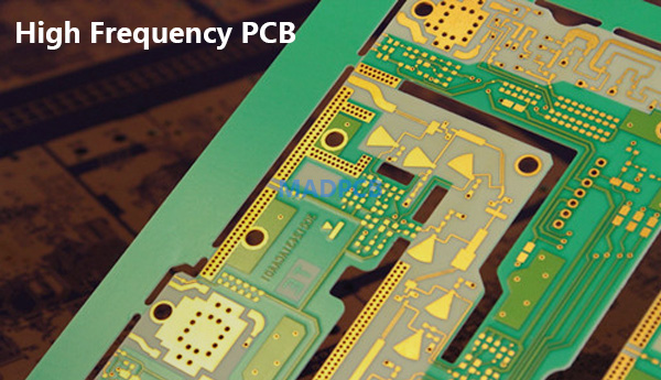
In today's fast-paced technological landscape, high-frequency printed circuit board (PCB) design plays a crucial role in ensuring accurate signal transmission and reliable performance for a wide range of applications. Whether you're working with analog signals, digital signals, or RF signals, considerations such as ground planes, material selection, component placement, and transmission line design are essential to achieve optimal signal integrity. In this article, we will explore key tips and best practices for designing high-frequency PCBs, including high-frequency circuit materials and techniques to reduce crosstalk and ensure signal transmission.

Understanding High-Frequency Signals:
High-frequency signals refer to those that operate at higher frequencies compared to traditional PCB designs. As frequencies increase, shorter signal rise and fall times become critical, and signal integrity becomes more challenging to maintain. Therefore, designing a high-frequency PCB requires special attention to minimize signal degradation, reflections, and noise interference.
Material Selection for High-Frequency PCBs:
Choosing the right materials is crucial for high-frequency PCB design. Consider using specialized high-frequency PCB materials such as PTFE-based or ceramic-filled hydrocarbon laminates like Rogers and Arlon, which offer low dielectric loss and improved electrical properties at higher frequencies. These materials provide better signal propagation and eliminate signal loss caused by high-frequency harmonics.
Ground Planes for High-Frequency PCBs:
Ground planes are an integral part of high-frequency PCB design. Maintaining a solid ground plane beneath signal lines and components helps to reduce unwanted radiation and minimizes noise coupling. Use dedicated ground planes for each signal layer to isolate analog, digital, and RF signals. Ensure that ground planes are uninterrupted and provide a low-impedance path for return currents.
Transmission Line Design:
Transmission lines are essential to ensure consistent signal integrity. For high-frequency signals, controlled impedance traces are critical to minimize signal reflections and maintain signal quality. Use microstrip or stripline transmission lines based on the layer stackup and design constraints. Proper impedance matching with characteristic impedance helps to achieve optimal signal transmission and reduce signal degradation.
Crosstalk Reduction Techniques:
Crosstalk is a common issue in high-frequency PCBs, where unwanted electromagnetic coupling between neighboring traces affects signal quality. To reduce crosstalk, increase spacing between signal traces, use ground planes between adjacent signal layers, and utilize shielding techniques such as using guard traces or ground vias. Crosstalk can also be minimized by considering differential signaling and employing differential pairs in high-speed/high-frequency designs.
Component Placement for Signal Integrity:
Strategic component placement is crucial for high-frequency PCBs. Place critical components, such as RF components or high-speed interface ICs, close to their corresponding signal entry points. Minimize trace lengths and avoid sharp bends to reduce parasitic capacitance and inductance, which can lead to signal degradation. Group components based on their functionality to minimize the trace length between them and promote efficient signal flow.
Signal Integrity Analysis:
Perform rigorous signal integrity analysis using simulation tools such as SPICE or electromagnetic simulators like HFSS or CST Microwave Studio. These tools help identify potential issues such as signal reflections, crosstalk, or impedance mismatch before production, allowing for necessary design modifications. Simulation-based analysis ensures that the high-frequency PCB design meets the desired performance requirements.
Power Integrity Considerations:
Ensuring stable power distribution is vital for high-frequency PCBs. High-frequency circuits often have unique power requirements, including the use of power planes and bypass capacitors to minimize power supply noise and voltage fluctuations. Proper decoupling capacitor placement near power pins of ICs is essential to suppress high-frequency noise and maintain signal integrity.
Thermal Management:
High-frequency circuits can generate significant heat. Efficient thermal management is crucial to prevent performance issues and ensure the reliability of the PCB. Consider heat sinks, thermal vias, or even active cooling techniques when designing high-power/high-frequency PCBs.
Prototyping and Testing:
Prototyping and testing are integral parts of any PCB design process. Fabricate and test prototypes to validate your high-frequency PCB design. Use spectrum analyzers, oscilloscopes, and vector network analyzers to measure signal quality, impedance, crosstalk, and other high-frequency parameters. Iterate on your design based on the results to achieve the desired performance.
In summary, designing a high-frequency PCB requires careful consideration of various aspects, including material selection, ground planes, transmission lines, component placement, and signal integrity analysis. By implementing these tips and best practices, you can ensure reliable signal transmission, reduce crosstalk, and maintain excellent performance in high-frequency applications. With the right techniques and materials combined with diligent testing and analysis, your high-frequency PCBs can meet the demanding requirements of today's advanced technologies.