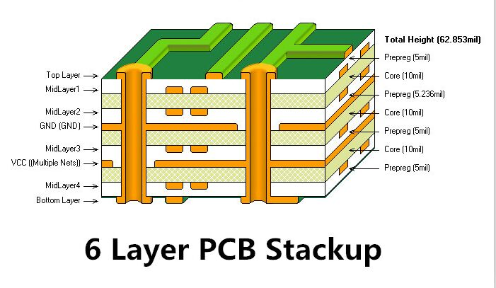
With the rapid evolution of electronics, the demand for advanced circuit boards has significantly increased. To ensure optimal performance of electronic devices, the arrangement of different layers within a printed circuit board (PCB) is crucial. This arrangement, known as a PCB stackup, plays a vital role in the device's functionality and performance.
In this article, we will explore the benefits and significance of a standard 6-layer PCB stackup. We will discuss the importance of each layer and how it impacts signal integrity and design efficiency.

A PCB stackup refers to the arrangement of different layers within a PCB to meet specific design requirements. These layers come together to form a stack, serving as the foundation of an electronic device. In a standard 6-layer PCB stackup, there are typically four signal layers and two inner planes, including a ground plane and a power plane.
Signal layers are critical components in a 6-layer PCB stackup. These layers are responsible for transmitting high-speed signals, such as data and other essential information. Maintaining proper impedance control is crucial to ensure accurate signal transmission and predictable behavior. Failure to manage impedance correctly can lead to signal degradation, reflections, and ultimately, compromised signal integrity.
In addition to signal layers, a 6-layer PCB stackup also includes two internal layers. Positioned between the signal layers, these internal layers serve multiple purposes. They provide additional routing options, allowing designers to efficiently connect various components and critical traces. Moreover, the internal layers play a significant role in directing signal paths and reducing interference from noise.
The top and bottom layers of a 6-layer PCB stackup hold significant importance in the overall design. The top layer accommodates essential components like integrated circuits, connectors, and surface-mounted devices. Proper component placement on this layer is crucial for signal integrity and maintaining design efficiency.
The bottom layer primarily serves as a connection to the ground. It provides a stable reference plane for a low-impedance return path.
Designing a 6-layer PCB stackup requires careful consideration of various factors. Proper layer ordering is essential to achieve desired electrical performance and avoid potential signal integrity issues. Utilizing custom services in PCB design offers numerous benefits. These include improved layer arrangements, precise routing for consistent signals, and overall design quality enhancements.
A standard 6-layer PCB stackup offers several advantages compared to simpler PCB designs. Effective management of signal layers, ground planes, and power planes significantly enhances signal integrity, reduces noise interference, and results in improved device performance and immunity to external disturbances. Furthermore, incorporating internal layers and optimizing the top and bottom layers allows for increased component density and overall design optimization.
A well-designed PCB stackup should never be underestimated in the realm of electronics. In standard 6-layer PCBs, careful consideration should be given to signal layers, ground planes, power planes, and internal layers to ensure their proper functionality and reliability. By understanding the importance of each layer within the stackup and considering critical design factors, engineers and PCB designers can enhance their designs and meet the requirements of modern electronic devices.
1. What is the meaning of PCB stackup?
PCB stackup refers to the arrangement of different layers within a printed circuit board (PCB) to meet specific design requirements. It involves strategically positioning layers to optimize the circuit's performance, including factors such as signal integrity, impedance control, thermal dissipation, and electromagnetic compatibility (EMC).
2. Why are signal layers important in a 6-layer PCB stackup?
Signal layers are crucial for transmitting high-speed signals and maintaining signal integrity. Proper impedance control ensures accurate signal transmission and prevents degradation, reflections, and compromised signal integrity.
3. What is the role of internal layers in a 6-layer PCB stackup?
Internal layers provide additional routing options and facilitate efficient connections between components. They also direct signal paths and help reduce noise interference.
4. How do top and bottom layers contribute to a 6-layer PCB stackup?
The top layer accommodates critical components, while the bottom layer provides a stable reference plane for a low-impedance return path.
5. What are the benefits of a standard 6-layer PCB stackup?
A standard 6-layer PCB stackup offers enhanced signal integrity, reduced noise interference, increased component capacity, and improved design efficiency, resulting in better overall device performance.