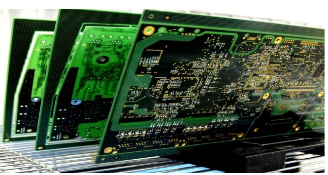
Welcome! If you've ever explored how your high-power LED lights function or how your device responds so quickly to a command, you're at the right place! Here, we demystify Custom Metal Core LED Light Metal Circuit Board PCB Fabrication. It's not as complex as it sounds, trust me!

PCBs, or Printed Circuit Boards, are virtually the backbone of every electronic device. Described as the city plan of your devices, they're an intricate network of pathways that electrically connect different components.
Diving deeper into PCBs, we encounter various types, including the crucial Metal Core PCBs. These PCBs have excellent thermal conductivity, effectively dissipating heat and keeping your devices cool under pressure. PCBs
These basic types consist of a single layer of base material coated with a thin layer of metal, housed ideally in low-power consumption circuits.
Double-sided PCBs up the ante, with metallic layers on both sides and through-holes to electrically connect different layers.
Multilayer PCBs take complexity to a new level, layering up to 12 layers all connected with special adhesives. Like a bustling city, these layers communicate and transfer heat efficiently, keeping the electronic components cool and functioning.
As the name suggests, these are the steadfast and stable components, often found in devices like TVs where the form factor remains unchanged.
Flex PCBs or flexible LED circuit boards are transformative and adaptative variants and can bend and fit into space constraints where rigid PCBs can't step in.
With the basics in hand, let's now dive into the specialty arena of fabrication, specifically in the creation of Metal Core PCBs for LED Lights.
The process of customizing LED circuit board design is instrumental in ensuring both innovation and efficiency. Why settle for less when you can actualize peak performance and minimize wastage with a customized touch?
Understanding the subtleties of the PCB fabrication process brings appreciation for the complex simplicity of PCBs. Specific details, like the circuit board design being mapped using Gerber files, come into play here.
The journey from the blueprint to printing is the first stage where PCBs take form. A photo-reactive coating is applied post-design.
Next, the unwanted copper is meticulously etched out of the design, etching the path our current will journey, under careful supervision.
Precision is key as holes are drilled to accommodate the various components and interconnections between PCB layers.
Finally, electronic components find their place and are meticulously soldered in. With that, you get a functioning and efficient PCB!
Thus, the world of Custom Metal Core LED Light Circuit Board PCB Fabrication brings together engineering, art, and customization. It's a realm where function meets form and moving forward towards an electronic future becomes a distinct possibility.
These creations utilize a metal core or an aluminum base to enhance power function, efficiently dissipate heat, convert a high-power LED light into an eco-friendly power source, and promote the production of more Aluminum PCB LEDs.
A Printed Circuit Board, commonly referred to as PCB, serves as both a mechanical foundation and an electrical pathway for the components of an electronic device. It acts as a base for any electronic configuration and functions by directing current around its surface via a network of copper pathways. Essentially, PCBs act as the nervous system for an electronic component, connecting, supporting, and facilitating communication between different components of an electrical device, thereby regulating their function, performance, and interaction.
The specifics of an electronic device heavily influence the design, architecture, and complexity of its corresponding PCB. Each device requires unique power, component configurations, and functionality, creating an inherent need for customized PCBs. Moreover, the configuration of the circuit - including the positioning and interconnection of components and layers - plays a crucial role in PCB's efficiency, signal quality, and other performance aspects. Thus, the notion of a 'one-size-fits-all' with respect to PCBs is impractical.
While designing a PCB involves intricate work, yes, it is entirely possible to create one at home, especially for hobbyists and students. It requires certain competencies, such as an understanding of electronics, circuits, layout designs, and software tools for PCB design. To equip yourself, you can take advantage of several online tutorials, courses, and material that can help you become proficient with the process. Besides, you need to have access to the appropriate materials, tools, and software, including PCB design software, copper boards, and etching solutions for the actual production.
The manufacturing process of PCBs traditionally involved some materials and procedures harmful to the environment, contributing to pollution. However, with increasing awareness about environmental issues, many strides have been made to make PCB production more eco-friendly. Manufacturers today are inclined towards using recyclable materials, reducing waste in the production process, and minimizing energy consumption. Nevertheless, the level of eco-friendliness varies greatly from one manufacturer to another, and it's essential to choose a manufacturer that aligns with your ecological standards.
Multi-layer PCBs are highly intricate and can consist of various layers of substrate and copper. To connect these layers, a design technique called 'via' (Vertical Interconnect Access) is used. Vias are essentially holes that are sometimes filled with conductive material, allowing electrical connections between different PCB layers. There are two types of vias: through-hole vias that pass through the entire board and blind/buried vias that connect only certain layers without running through the whole board. This effective technique facilitates compact designs without compromising functionality and performance.