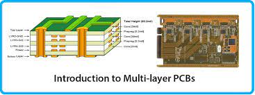
Multilayer PCBs (Printed Circuit Boards) are electronic circuit boards that consist of multiple layers of conductive traces and insulating material stacked together. These boards are commonly used in complex electronic devices and applications where a high degree of circuit density and functionality is required. Here are some of the key features of multilayer PCBs:

Multiple Layers: As the name suggests, multilayer PCBs have more than two layers of conductive traces and insulating material. They can have anywhere from four to dozens of layers, depending on the complexity of the circuitry.
High Component Density: Multilayer PCBs allow for a higher density of electronic components and interconnections compared to single-layer or double-layer PCBs. This makes them suitable for compact and densely populated electronic devices.
Improved Signal Integrity: The multiple layers in a multilayer PCB provide a better environment for routing high-frequency signals and reducing electromagnetic interference (EMI). Properly designed ground and power planes can help manage signal integrity.
Enhanced Power Distribution: Multilayer PCBs can include dedicated power and ground planes, which help distribute power efficiently throughout the board. This is important for stable and reliable operation of electronic circuits.
Reduced Crosstalk: The separation of signal traces on different layers can reduce crosstalk (unwanted interference) between adjacent traces, which is crucial for maintaining signal quality, especially in high-speed digital circuits.
Complex Routing: Multilayer PCBs offer more routing options, allowing designers to create intricate and complex circuits with minimal space constraints. This flexibility is essential for advanced electronic devices.
Miniaturization: Multilayer PCBs enable the miniaturization of electronic devices because they allow designers to pack more functionality into a smaller footprint.
Increased Reliability: The use of multiple layers and robust materials enhances the overall reliability and longevity of multilayer PCBs. This is particularly important for mission-critical applications.
Thermal Management: Multilayer PCBs can incorporate thermal vias and heatsinks to efficiently dissipate heat generated by electronic components. This is crucial for preventing overheating and ensuring the reliability of the circuitry.
Improved Noise Immunity: Multilayer PCBs can provide better noise immunity by separating analog and digital signal traces, reducing interference between them.
Reduced Electromagnetic Radiation: Properly designed multilayer PCBs can help reduce electromagnetic radiation, which is important for compliance with regulatory standards and preventing interference with other nearby electronic devices.
Design Complexity: Designing multilayer PCBs can be more complex and time-consuming than single or double-layer PCBs. It requires specialized software and expertise to ensure proper layer stacking, signal routing, and manufacturing considerations.
Cost: Multilayer PCBs are typically more expensive to manufacture than simpler PCBs due to the added complexity and manufacturing steps involved.
Overall, multilayer PCBs are a crucial component in modern electronics, enabling the development of advanced and compact electronic devices with enhanced performance and functionality. Their design and manufacturing require careful consideration of various factors to meet the specific requirements of a given application.