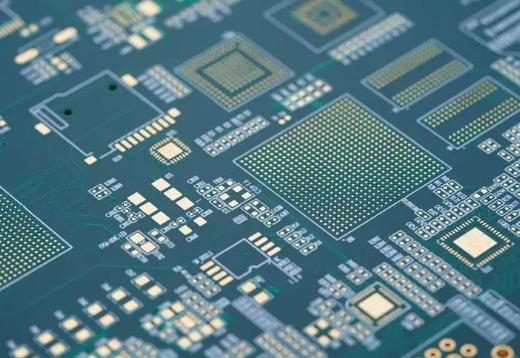
High-Density Interconnect (HDI) PCBs (Printed Circuit Boards) often employ various types of vias to enable the routing of signals and power between different layers of the PCB. Two common types of vias used in HDI PCBs are through vias and blind vias. Let's compare these two types:

1.Purpose and Function:
Through Vias: Through vias, as the name suggests, extend completely through all layers of the PCB. They are used to establish electrical connections between all layers of the board, from the top to the bottom. Through vias are essential for multilayer PCBs as they enable vertical signal and power distribution.Blind Vias: Blind vias, on the other hand, connect only one or more specific layers, without penetrating the entire PCB. They are designed to connect an outer layer to one or more inner layers of the PCB, allowing for more complex routing options and reducing the need for through-hole drilling.
2.Manufacturing Complexity:
Through Vias: Manufacturing through vias is relatively straightforward since they penetrate all layers, making them suitable for standard fabrication processes. They are drilled and plated after the layer stack-up is complete.
Blind Vias: Blind vias require more complex manufacturing processes, including laser drilling or controlled-depth drilling, to connect specific layers. This complexity can increase the overall cost of PCB fabrication.
3.Density and Space Efficiency:
Through Vias: Through vias take up valuable real estate on all layers of the PCB, which can limit the available space for routing traces and components, particularly in densely populated designs.
Blind Vias: Blind vias are space-efficient because they only connect specific layers, leaving more room for traces, components, and signal routing on other layers. This makes them ideal for high-density designs.
4.Signal Integrity:
Through Vias: Through vias can potentially introduce more signal integrity issues due to their longer path and larger impedance discontinuities. Proper design and impedance control are crucial to mitigate these effects.
Blind Vias: Blind vias can help reduce signal integrity issues because they have shorter paths and fewer impedance discontinuities. However, their impact on signal integrity still needs to be considered in the PCB design.
5.Cost:
Through Vias: Through vias are generally more cost-effective to manufacture because they are part of the standard fabrication process for multilayer PCBs.
Blind Vias: Blind vias can increase manufacturing costs due to the added complexity and the need for specialized equipment.
In summary, the choice between through vias and blind vias in HDI PCBs depends on the specific design requirements, space constraints, signal integrity considerations, and budget constraints. Through vias are simpler and more cost-effective, while blind vias offer greater space efficiency and can help address signal integrity concerns in high-density designs. Designers should carefully evaluate their project's needs to make an informed decision.
Get more knowledge about Comparison between through vias and blind vias in HDI PCBs please refer to Rigaopcb:https://www.rigaopcb.com/