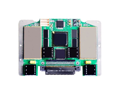
A multilayer printed circuit board (PCB) is an advanced type of PCB that consists of multiple layers of copper traces, insulating material, and vias (plated holes) that connect these layers. Multilayer PCBs are commonly used in complex electronic devices and applications where space is limited and signal integrity is critical. Here are the basics of multilayer PCBs:

1.Layer Structure: A multilayer PCB comprises multiple layers of conductive traces and insulating material stacked together. The number of layers can vary from four to many more, depending on the complexity of the design.
2.Copper Layers: The conductive layers are typically made of copper. These layers serve as the pathways for electrical signals to travel between components on the board.
3.Insulating Layers (Substrates): Between each copper layer, there is an insulating material known as a substrate or dielectric. Common materials include FR-4 (a type of fiberglass-reinforced epoxy), polyimide, and PTFE (Teflon).
4.Vias: Vias are plated holes that connect different layers of the PCB. They allow electrical connections to be made between traces on different layers, helping to route signals efficiently and reduce the overall footprint of the board.
5.Through-Hole Vias: These vias penetrate through all layers of the PCB, connecting traces on different sides of the board. They are commonly used for power and ground connections.
6.Blind Vias: Blind vias connect an outer layer to one or more inner layers, but they do not go through the entire board. These are used to route signals between specific layers while minimizing signal interference.
7.Buried Vias: Buried vias connect inner layers without extending to the outer layers. They offer additional routing options while maintaining a cleaner outer appearance.
8.Solder Mask: A protective layer called solder mask is applied to the top and bottom surfaces of the PCB. It covers the copper traces and prevents solder from unintentionally bridging connections.
9.Silkscreen: A layer of ink-based marking called silkscreen is applied on the top and/or bottom of the PCB. It includes component labels, reference designators, and other information to aid in assembly and troubleshooting.
10.Design Considerations: When designing a multilayer PCB, factors like signal integrity, power distribution, and thermal management become more critical due to the increased complexity. Proper ground planes, signal routing, and layer stackup are crucial for maintaining performance and reliability.
11.Manufacturing Process: The manufacturing process for multilayer PCBs involves laminating alternating layers of copper and insulating material under heat and pressure. The layers are then drilled and plated to create vias, followed by additional processing steps like solder mask application, surface finish, and silkscreen printing.
12.Applications: Multilayer PCBs are used in various applications, including high-speed digital circuits (such as in computers and networking equipment), telecommunications, aerospace, automotive electronics, medical devices, and more.
In summary, multilayer PCBs offer increased complexity and flexibility compared to single or double-sided PCBs, making them suitable for advanced electronic designs requiring compact form factors and enhanced performance.
Get more knowledge about What are the basics of multilayer PCB please refer to Rigaopcb:https://www.rigaopcb.com/