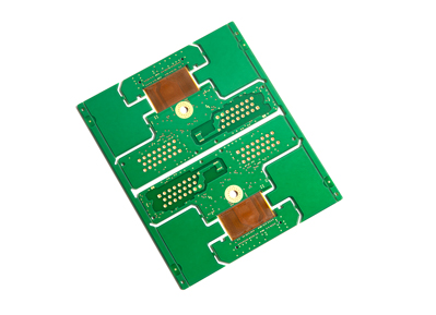
PCB (Printed Circuit Board) manufacturing capabilities encompass a wide range of processes and technologies involved in the fabrication of PCBs. This comprehensive guide will provide an overview of the key aspects and steps involved in PCB manufacturing, including design considerations, materials, manufacturing processes, and quality control.

1.Design Considerations:
PCB Layout: The design process involves creating a layout that determines the placement and routing of components and traces on the PCB.
Design for Manufacturing (DFM): Consider DFM guidelines to ensure that the design is optimized for manufacturing processes, such as minimizing the number of layers, avoiding complex shapes, and adhering to minimum clearances.
Design for Testability (DFT): Implementing test points, such as test pads or vias, to facilitate testing and troubleshooting during the manufacturing and assembly stages.
2.Materials:
Substrate Material: The most common substrate material is FR-4, a glass-reinforced epoxy laminate. Other materials like polyimide (flex PCBs) or metal core (MCPCB) may be used based on specific requirements.
Copper Foil: Copper is laminated onto the substrate material in various thicknesses, typically measured in ounces (e.g., 1 oz, 2 oz, etc.).
Soldermask: A protective layer applied over the copper traces to prevent solder bridges and protect against environmental factors.
Silkscreen: A layer for component markings, including reference designators, part numbers, logos, and other essential information.
3.Manufacturing Processes:
PCB Prototyping: Involves the production of a small batch of PCBs for design verification and testing purposes before mass production.
PCB Production: The mass manufacturing process typically involves the following
steps:
Inner Layer Core Preparation: Prepreg layers are sandwiched between copper foils, and the stack is pressed together to form the inner core.
Imaging: A photosensitive film called a photoresist is applied over the copper layers, and a photomask is used to expose the desired circuit pattern.
Etching: Chemical etching removes the unwanted copper from the exposed areas, leaving behind the desired copper traces.
Lamination: Multiple layers are stacked together, and heat and pressure are applied to bond them into a single multilayer PCB.
Drilling: Precision drills create holes for component mounting and interconnections.
Plating: Copper or other metals are plated onto the hole walls to establish electrical connections between layers.
Soldermask and Silkscreen Application: Protective soldermask and component marking layers are applied to the PCB.
Surface Finish: The final coating applied to the exposed copper pads to protect against oxidation and facilitate soldering.
Electrical Testing: Various tests, including continuity, impedance, and isolation testing, are conducted to ensure the PCB's functionality.
PCB Separation: The larger PCB panel is cut into individual PCBs.
Final Inspection: Visual inspection and quality control checks are performed to ensure the PCBs meet the required specifications.
4.Advanced Manufacturing Techniques:
High-Density Interconnect (HDI): Used for compact designs, HDI PCBs incorporate microvias, buried vias, and sequential build-up layers (SBU) to achieve higher routing densities.
Multilayer PCBs: PCBs with more than two layers, facilitating complex designs and higher integration of components.
Flex PCBs: Flexible PCBs that can bend or twist, suitable for applications with space or weight constraints.
Controlled Impedance: Precision manufacturing techniques to achieve specific impedance values for high-speed signal integrity.
5.Quality Control:
Automated Optical Inspection (AOI): Automated systems scan the PCBs for defects, including missing components, misalignment, and soldering issues.
Electrical Testing: PCBs undergo functional testing to ensure proper functionality and adherence to electrical specifications.
X-ray Inspection: X-ray machines are used to inspect hidden solder joints, vias, and internal layers for defects and quality issues.
Reliability Testing: PCBs may undergo various reliability tests, such as thermal cycling, vibration testing, and accelerated aging, to assess their performance under different conditions.
Certifications and Standards: Manufacturers may comply with industry standards such as IPC-A-600 (Acceptability of Printed Boards) and IPC-6012 (Qualification and Performance Specification for Rigid Printed Boards) to ensure high-quality PCB production.
6.Additional Services:
PCB Assembly: Some PCB manufacturers also offer PCB assembly services, where they populate the PCBs with components according to customer requirements.
Prototyping: Manufacturers may provide prototyping services to produce a small batch of PCBs for initial testing and validation.
Design Services: Some manufacturers have in-house design teams that can assist in PCB layout and design optimization.
It's important to note that PCB manufacturing capabilities can vary between manufacturers. Factors such as the complexity of the design, the number of layers, and the desired specifications may impact the manufacturing options available. It is recommended to consult with PCB manufacturers to understand their specific capabilities and processes to ensure they meet your project requirements.
By following these guidelines and working closely with a reputable PCB manufacturer, you can leverage their manufacturing capabilities to produce high-quality PCBs that meet your specific design requirements.
Get more knowledge about PCB Manufacturing Capabilities please refer to Rigaopcb:https://www.rigaopcb.com/