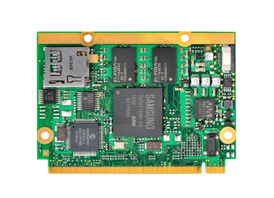
Designing a multilayer pcb requires careful consideration of various factors to ensure optimal performance, reliability, and manufacturability. Here is a comprehensive guide to multilayer PCB design best practices:

1.Plan the Layer Stackup:
Determine the number of layers required based on the complexity of the circuit and its components.
Consider signal integrity, power distribution, and thermal management requirements.
Follow industry standards for layer stackup, such as using ground and power planes, signal layers, and routing layers.
2.Signal and Power Integrity:
Group signals based on their characteristics (high-speed, low-speed, analog, digital) to minimize interference.
Use appropriate impedance control techniques, like controlled impedance traces, to maintain signal integrity.
Ensure proper decoupling capacitor placement to minimize power supply noise.
3.Component Placement:
Strategically place components to reduce signal path lengths, minimize noise, and optimize thermal dissipation.
Group related components together for better signal flow and shorter traces.
Consider the mechanical aspects, such as component height and clearance, to ensure proper assembly and fitting.
4.Routing Guidelines:
Follow design rules provided by the manufacturer and industry standards.
Minimize trace lengths and use appropriate widths to maintain signal integrity and impedance matching.
Separate high-speed and low-speed signals to prevent interference.
Use differential pair routing for high-speed signals to improve noise immunity.
Keep sensitive analog traces away from noisy digital signals.
5.Power and Ground Planes:
Incorporate solid ground and power planes to provide low impedance return paths and efficient power distribution.
Use multiple power and ground planes to separate different voltage levels and reduce noise coupling.
Avoid splitting planes whenever possible, as it can create return path issues.
6.Thermal Management:
Consider thermal dissipation requirements and place components accordingly.
Use thermal vias to connect heat-generating components to internal and external copper layers for better heat dissipation.
Distribute thermal vias evenly to maintain a uniform temperature across the PCB.
7.EMI/EMC Considerations:
Implement proper grounding techniques to minimize electromagnetic interference (EMI).
Place filtering components, such as capacitors and inductors, close to the noise source to suppress EMI.
Use shielding techniques, like ground planes and copper pour, to minimize electromagnetic emissions.
8.Design for Manufacturability:
Adhere to design rules and guidelines provided by the manufacturer to ensure manufacturability.
Maintain proper spacing between traces and pads to prevent short circuits during manufacturing.
Avoid complex and tight geometries that may increase the risk of fabrication errors.
Perform design rule checks (DRC) and design for test (DFT) analysis to identify and rectify potential manufacturing issues.
9.Documentation and Collaboration:
Create comprehensive design documentation, including schematic diagrams, layout files, and fabrication notes.
Clearly annotate design considerations, constraints, and special requirements for better collaboration with manufacturers and assembly teams.
10Prototyping and Testing:
Build a prototype and perform thorough functional and electrical testing to validate the design.
Use tools like oscilloscopes, logic analyzers, and network analyzers to verify signal integrity and performance.
Iterate the design based on the test results and optimize as necessary.
Remember that multilayer PCB design can be complex, and it is crucial to continuously learn and stay updated with the latest industry practices and standards. Collaboration with experienced PCB designers and manufacturers can also greatly enhance the quality of your designs.
Get more knowledge about Multilayer PCB Design please refer to Rigaopcb:https://www.rigaopcb.com/