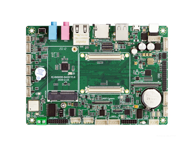
Manufacturing multilayer PCBs involves several steps, from design transfer to final assembly. Here's a step-by-step guide to manufacturing multilayer PCBs:

1.Design Transfer:
Start with a completed PCB design in electronic format (e.g., Gerber files, ODB++ files) generated from your PCB design software.
Prepare the design files, including the necessary layers (signal, power, ground, solder mask, silkscreen, etc.), drill files, and any additional documentation.
2.Panelization:
The individual PCB designs are often combined into a panel for efficient manufacturing and handling.
Determine the panel size and arrange multiple PCB designs within the panel, considering factors like manufacturing requirements, cost, and panel utilization.
Add fiducial marks and tooling holes to the panel for alignment and precise manufacturing.
3.Material Selection:
Choose the appropriate PCB material based on the design requirements (e.g., FR-4, high-frequency laminates).
Consider factors such as dielectric constant, thermal conductivity, and mechanical strength to ensure the material meets the desired specifications.
Select the copper thickness for the inner and outer layers (e.g., 1 oz, 2 oz) based on the current carrying capacity and manufacturing feasibility.
4.Layer Stackup Design:
Determine the layer stackup based on the number of layers required for your design.
Define the arrangement of signal layers, power planes, and ground planes, considering signal integrity, power distribution, and impedance control.
Determine the thickness of each layer and the overall PCB thickness.
Specify the prepreg and core thicknesses for each layer in the stackup.
5.Inner Layer Processing:
Start with the inner layers of the PCB stackup.
Cut the copper-clad laminate sheets to the required size.
Clean the copper surfaces and apply a layer of photosensitive material (photoresist) to both sides.
Expose the inner layers to UV light through a photomask to transfer the desired circuit pattern.
Develop and etch the inner layers to remove unwanted copper and reveal the circuit traces.
Inspect the inner layers for any manufacturing defects.
6.Lamination and Pressing:
Prepare the inner layers, prepreg, and outer copper-clad laminate sheets for lamination.
Align and stack the layers according to the predetermined layer stackup.
Place the stack into a lamination press and subject it to heat and pressure.
The heat and pressure bond the layers together, melting the prepreg material to create a solid multilayer PCB.
7.Drilling:
Drill the required holes (vias and through-holes) in the laminated PCB stack.
Use computer-controlled drilling machines to ensure accurate hole placement and size.
Clean the drilled PCB stack to remove any debris or residues.
8.Plating:
The drilled holes are plated with a conductive material (usually copper) to create the required electrical connections between layers.
Initially, the holes are chemically cleaned and activated.
They are then electroplated with a thin layer of copper.
The excess copper is plated over to ensure the holes are completely filled.
The surface of the PCB is also plated with a protective layer (e.g., tin, gold) to prevent oxidation.
9.Outer Layer Processing:
Apply a layer of photosensitive material (photoresist) to the outer layer copper surfaces.
Expose the outer layers to UV light through a photomask to transfer the desired circuit pattern.
Develop and etch the outer layers to remove unwanted copper and define the final circuit traces.
In summary, the manufacturing process of multilayer PCBs involves design transfer, panelization, material selection, layer stackup design, inner layer processing, lamination and pressing, drilling, plating, and outer layer processing. Each step plays a crucial role in creating a reliable and high-performance multilayer PCB. By following best practices and guidelines, designers can ensure successful manufacturing and assembly of their multilayer PCB designs.
Get more knowledge about The Step-by-Step Guide to Manufacturing Multilayer PCBs please refer to Rigaopcb:https://www.rigaopcb.com/