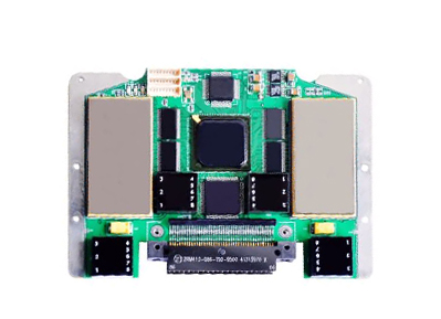
Designing multilayer PCBs requires careful planning and adherence to best practices to ensure optimal performance and reliability. Here are some guidelines and best practices to consider when designing multilayer PCBs:

1.Layer Stackup:
Determine the required number of layers based on the complexity of the circuit and signal integrity requirements.
Use a balanced layer stackup to ensure even distribution of signal and power planes across the PCB.
Place power and ground planes adjacent to each other for effective decoupling and noise reduction.
Minimize the number of signal layers crossing over split planes to avoid signal integrity issues.
2.Signal and Power Integrity:
Group components based on their signal requirements and allocate appropriate signal layers.
Use dedicated power and ground planes to provide low impedance paths for power distribution.
Add decoupling capacitors near high-speed ICs to minimize power noise and maintain signal integrity.
Follow proper high-speed design techniques like impedance control, controlled impedance traces, and length matching for critical signals.
3.Routing Considerations:
Minimize trace lengths to reduce signal delay and interference.
Use wider traces for high-current or power-carrying signals to minimize resistance and heat generation.
Separate analog and digital signals to minimize noise coupling.
Follow proper spacing and clearance guidelines to prevent crosstalk and ensure manufacturability.
4.Thermal Management:
Add thermal vias to connect copper planes to inner layers for effective heat dissipation.
Place heat-generating components near the edges of the PCB to facilitate heat dissipation.
Consider adding heatsinks or thermal pads for components that require extra cooling.
5.Component Placement:
Group components based on their functionalities and interconnections.
Place critical components closer to each other to minimize trace lengths and reduce signal degradation.
Consider component height and clearance requirements to avoid interference with neighboring layers or components.
6.Manufacturing and Assembly:
Follow design rules and guidelines provided by the PCB manufacturer to ensure manufacturability.
Use standard component footprints and keep components within recommended tolerances.
Provide adequate spacing for solder mask and silkscreen to avoid smearing or overlapping.
Perform a design rule check (DRC) to catch any potential errors before fabrication.
7.Documentation and Collaboration:
Create comprehensive and well-organized design documentation including schematics, layer stackup, and fabrication files.
Collaborate with PCB fabricators and assembly houses throughout the design process to address any manufacturing constraints.
Remember to use PCB design software that provides features for designing multilayer PCBs, such as layer stackup tools, impedance calculators, and design rule checks. Additionally, always verify your design with simulation tools and seek feedback from experienced PCB designers to ensure a successful multilayer PCB design.
Get more knowledge about Designing Multilayer PCBs please refer to Rigaopcb:https://www.rigaopcb.com/